![]() Intel’s foundry arm that doesn’t officially exist has a new customer, Netronome. The maker of networking chips is moving from TSMC’s 65nm process to the bleeding edge Intel 22nm tri-gate process, likely with some other goodies attached too.
Intel’s foundry arm that doesn’t officially exist has a new customer, Netronome. The maker of networking chips is moving from TSMC’s 65nm process to the bleeding edge Intel 22nm tri-gate process, likely with some other goodies attached too.
In case you are not familiar with Netronome, they are the only company with a license to make CPUs based on the Intel IXP architecture. Intel used to make network co-processors to plug in to Xeons, but has since handed that over to Netronome. The older IXP2800 chip, the current NFP-32xx line, and the upcoming and as yet un-revealed 22nm parts are now in the hands of another company.
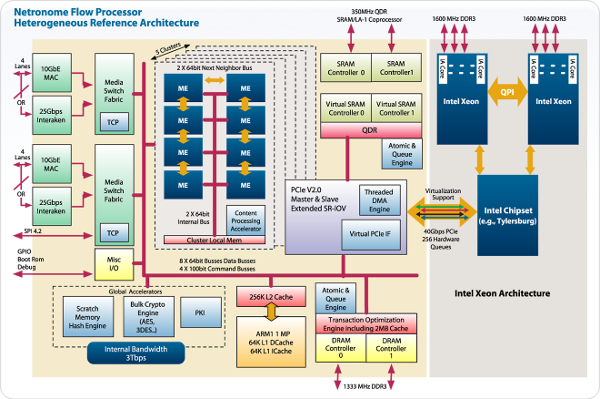
The architecture of the chip is meant for low latency network throughput, it is basically a big array of simple units, call them MicroEngines (MEs), cores, processors, or whatever, all strapped together with a high speed on-die interconnect. Surround it with fast memory, fast I/O, an ARM11 controller to keep everything moving in the same general direction, then slap accelerator blocks on as needed, and put a wide 40Gbps PCIe interface on it. There you have a complete network accelerator on a card ready to plug in to a PC server and compete with dedicated hardware. Note the Xeons at the right hand side, the IXP architecture is how Intel aims to play in the networking and switching space.
Netronome’s reference architecture diagram
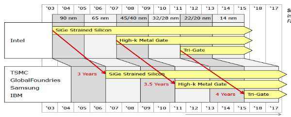
Upcoming Netronome processors will likely also complement Intel’s server CPUs, so it is in Intel’s best interest to keep them competitive. If OpenFlow/Software Defined Networking takes off, Intel is in a great position to supply half the building blocks of choice. Luckily, Netronome is the other half of the equation, so they aren’t complaining about Intel’s process lead either. The slide below from the last IDF, is a pretty good proxy for Netronome vs the competition in the process space. Chip architecture matters a lot in this space, but this kind of lead on the transistor level never hurts. Luckily, the most important piece of the puzzle is also currently exclusively tied to the 22nm process.
Key technologies and timelines
The biggest problem for CPUs like Netronome is I/O bandwidth, be it memory, network ports, or to a host system, bandwidth is always the key factor. As you can see from the architecture diagram above, the current chip will support eight 10Gbps lanes and a 40Gbps PCIe interface plus two DDR3 channels and two SDRAM channels. That is a lot of pins, a huge number, so it will be a board routing nightmare.
When you step up to the next generation of network processors like Netronome is about to launch, the bandwidth will need to increase by an order of magnitude or more. Memory hasn’t kept up that pace since DDR3 so what can a designer do? The obvious choice is to stack memory on the die or on package with an interposer, and connect the two through a rather silly width interface. IBM has done this without an interposer for the Power line for a while, but it is rather expensive, too expensive for mere mortals to buy.
Power 7+ drops production cost by a few orders of magnitude with an interposer, or it will when announced, but don’t expect that to be reflected in the MSRP. Worse yet, no one has publicly committed to offering such technology to foundry customers, but you see a few prototypes here and there. What is a small company to do, develop the tech on their own? HINT. Problem solved. 22nm is going to do very well for Netronome, very well indeed, but the key differentiator for them is not exactly where you might think it is.S|A
Charlie Demerjian
Latest posts by Charlie Demerjian (see all)
- What is Qualcomm’s Purwa/X Pro SoC? - Apr 19, 2024
- Intel Announces their NXE: 5000 High NA EUV Tool - Apr 18, 2024
- AMD outs MI300 plans… sort of - Apr 11, 2024
- Qualcomm is planning a lot of Nuvia/X-Elite announcements - Mar 25, 2024
- Why is there an Altera FPGA on QTS Birch Stream boards? - Mar 12, 2024

