![]() There is a lot of talk about the benefits of chip stacking, but only one company is doing it in volume, Xilinx. Luckily, one of their devices is showing off one feature that few talk about, component reuse, as well as the more common benefits.
There is a lot of talk about the benefits of chip stacking, but only one company is doing it in volume, Xilinx. Luckily, one of their devices is showing off one feature that few talk about, component reuse, as well as the more common benefits.
At Hot Chips 24, Xilinx’s Shankar Lakka gave a talk about their SSI technology, Stacked Silicon Interconnect to us mere mortals, and how it enables heterogenous SoCs. This is the technical way of saying that you can put a lot of different chips on an interposer to make a single completed unit that would otherwise be impossible to make with conventional methods.
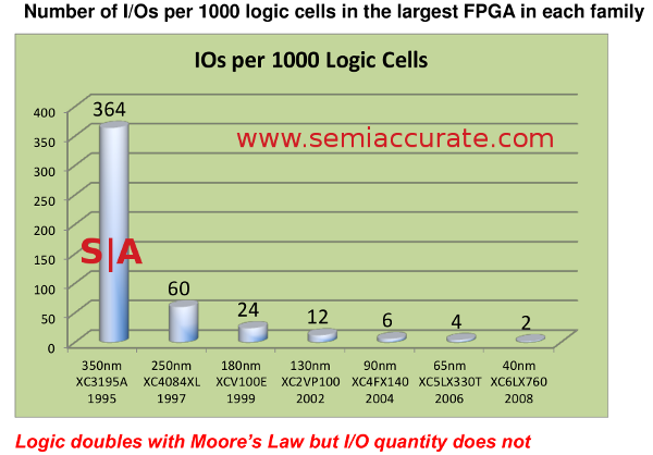
The problem in a nutshell, I/Os don’t scale well
The first problem is well known, call it being pad or bump bound. Moore’s law states that the transistor count of a microchip doubles every 18 months, but it doesn’t extend to the bumps and other interconnects that run to and from the chip. Those are built with much more conventional tools, a flip chip uses balls of solder that are orders of magnitude larger than the transistors to connect them to the substrate. The substrate in turn has to connect to the PCB, so those balls, pads, or similar technologies have to be vastly bigger than those.
Making them smaller is quite possible, but little things like actually building the device becomes far more problematic as features shrink. For yield reasons, you want them as large as possible. For everything else, you want them as small as possible. If you can’t make the device, the fact that it is an amazing design on paper is rather secondary.
There is an incredible amount of work that goes in to the whole process, from thermal modelling and stress analysis to financial planning, it is a critical part of modern IC development. If you do it right, things work out well, if you don’t, it can be disastrous. Remember this?
Then there is the problem of making the dies themselves. Big dies are great halos, and if you have a small market that will pay absurd amounts for a solution that they must have, you win. If you are selling against competing solutions with smaller dies, you are going to have a hard time making money. The rule of thumb is that yield goes down with the square of the die size, but there are a lot of mitigating factors, planned repairability and redundancy being a key ones. Then again, those too have tradeoffs, and larger dies also take longer to develop, simulate, test, and debug.
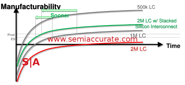
If only you could make a chip from multiple pieces, each optimized for a task, and put them all together in to one big chip with no losses, no extra power used for I/O, reusable components, and silicon scale interconnects, you could make a killer product. Better yet, imagine if you could use multiple copies of the same component for better yields, easier validation, and quick time to market. And that is what Xilinx is doing. As you can see from the graph below, it really does pay off to do multiple dies with an interposer.
How stacking affects manufacturing
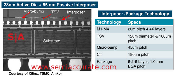
In their Virtex-7 HT FPGA, Xilinx uses all of this to do things that would be extremely difficult if not impossible to do in conventional ways. This device uses three FPGA dies and two dedicated SerDes dies on a single interposer. The FPGAs are on a process optimized for low power, the SerDes dies are built on another process that is more performance oriented, and all of it is mounted on a silicon interposer. Since that interposer is made from the same silicon as the dies, all of the wires can be made on a 65nm chip process and use 45µm microbumps vs 180µm C4 bumps to the substrate. Compare this to the 1mm pitch of the balls connecting it all to the to the PCB.
What it looks like in cross section
With this, the whole I/O:logic ratio as seen above moves much closer to the scaling curve defined by Moore’s Law than was possible before. The silicon on silicon nature of the interposer mitigates a lot of the thermal strain problems too, but assembly is much more problematic. That said, you can fit 16 times as many microbumps under a die as you can C4 bumps, I/O power drops proportionately, and you can make different dies on the most appropriate process instead of compromising all of it for a single large chip.
Xilinx is doing it all now in volume, you can buy a few different versions on the open market, so it looks to be a win for them. While the company did not talk about finances, cost, or yields, given the plethora of products they make that are using the tech, it looks to be profitable too. The entire Virtex-7 HT device has 2.8Tbps of bandwidth from 72 13Gb transceivers and 16 28Gb transceivers, but it only uses 650 I/Os. Compare that to any modern CPU, it is far far fewer pins for vastly higher net I/O bandwidth. If you could build a similar device on a monolithic chip, it would have far worse power consumption, less process optimization, and yields that would be a fraction of any of the five chips used here. I guess the take home message is that it works, works now, and the benefits are game changing, not evolutionary.S|A
Charlie Demerjian
Latest posts by Charlie Demerjian (see all)
- Qualcomm Is Cheating On Their Snapdragon X Elite/Pro Benchmarks - Apr 24, 2024
- What is Qualcomm’s Purwa/X Pro SoC? - Apr 19, 2024
- Intel Announces their NXE: 5000 High NA EUV Tool - Apr 18, 2024
- AMD outs MI300 plans… sort of - Apr 11, 2024
- Qualcomm is planning a lot of Nuvia/X-Elite announcements - Mar 25, 2024


