![]() LSI is the first SoC vendor to hit the magic 16-core mark for an ARM based phone chip, but the Axxia 5500 isn’t what you think. It does have 16 cores, is for cell phones, but it is aimed at the other side of a call, the base stations.
LSI is the first SoC vendor to hit the magic 16-core mark for an ARM based phone chip, but the Axxia 5500 isn’t what you think. It does have 16 cores, is for cell phones, but it is aimed at the other side of a call, the base stations.
The Axxia family is something we have told you about in its previous incarnation, the 3400 line, but there are some major changes that come with the new 5500 chips. From an overview standpoint, things may look quite similar, but under the hood almost everything is all new. Some of this is because LSI telegraphed chunks of this architecture at their AIS conference a few months ago and some because it conceptually is just a generational advance. Since the Axxia line is aimed at telecom carriers, a group that can be terribly averse to many types of radical change, this similarity is a good thing.
Meet the new chip, in some ways just like the old chip
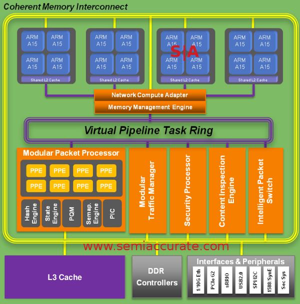
The first thing you may notice is that the Axxia 5500 line has up to four clusters of four ARM A15 cores all connected through the CCN-504 bus that LSI co-developed with ARM. This lets the CPUs maintain coherence over the main memory bus, but somewhat counter-intuitively, process control is done across the Virtual Pipeline Task Ring (VPTR). There are very good reasons to run management tasks over a completely separate bus, both for partitioning and fine grained process control.
If you look at it from the perspective of how the tasks are executed, this organization makes a lot of sense. Many of the tasks that the Axxia line was designed to execute do not just use a single core, they may take packets in across the Modular Packet Processor (MPP), decrypt the data on a crypto accelerator, authenticate with the security hardware, and then pass it to a CPU for more complex tasks. Having the VPTR controlling workflow simplifies things immensely because none of the functional units need to know anything about process control.
The VPTR knows what needs to be done where so the cores and accelerators don’t need to have that logic and overhead built in, much less do it in real time. State can be maintained separately from function in the Axxia 5500 family and this simplifies multi-unit tasks immensely. It also allows the device to be hard partitioned rather arbitrarily and irrespective of the code being run, so things can’t really break out of the sandbox they are placed in. Partitioning can be any number of cores, accelerators, or even the busses themselves, everything is controlled by a configuration file at boot, not running code. From that point, process flows are owned and controlled by the VPTR, and the code running can’t see any other flows or use their assigned resources. That gets telcos what they want, security and dedicated resources in potentially shared environments like big base stations.
These process flows can potentially utilize all 16 cores, the MPP, plus all of the accelerators to do their work, or be locked to a single piece. Like the previous 3400 family the bus is open to customers. LSI is open to putting in third party IP and hardware blocks as requested. Some telcos have DSP blocks they developed and want to use, others may have a digital front end they prefer, but all can be added to the 5500 if you buy enough. Unlike the older model, there is no option for a PowerPC core in this generation, it is ARM A15 cores only.
Accelerators available to the Axxia 5500 family are much the same as they were in earlier generation, but newer, faster, and with all the advances you would expect from newer silicon. The chip has an integrated 10GigE switch built in with 16 ports (160Gbps of bandwidth), think of this as a starting point. Networking can work with the MPP, it is a fully programmable network processing engine in itself, think primitives rather than stacks defined in hardware. There are additional engines to modulate traffic flow, check security, inspect packets for all sorts of things that annoy end users, and much more in the basic CPU.
Feeding all of this compute capability is four DDR3/1866 controllers, two for the main system and two are dedicated to the MPP. This is a fair chunk of memory bandwidth, but pales in comparison to what the ethernet can pull in. Luckily, the Axxia chips don’t have to store that data, they mainly check it, tweak it, and pass it along the wire as fast as possible. To manage this, the chip is aware of most networking and telco protocols like you would expect it to be, plus a bunch you probably have never heard of unless you design cellular hardware and software. If it doesn’t support what you want, you can always add a block of hardware to do it, modularity is nice that way.
In the end what you get is a chip that LSI claims will do 100% of wireless transport termination, backhaul aggregation, and packet processing in your choice of nine high fashion exterior finishes. It can crunch data at up to 50Gbps without using the CPUs at all, just the accelerators. If this isn’t enough, add whatever you require for your tasks, it is modular and uses standard ARM busses so it shouldn’t be too much of a chore. At the moment you can choose from two Axxia 5500 variants, the 16-core AXM5516 and the 12-core AXM5512, but many more are sure to follow. The architecture scales from 4 to 32 CPUs, so larger and smaller versions will not be long in coming. They are all 28nm devices, no die size, TDP, or fab was given but TMSC seems the likely candidate.
If you are wondering why LSI is making things so modular, there is a point to all of this other than someone liking custom hardware. One of the big headaches that carriers have is something called HetNet or Heterogeneous Network. If you think about it, to run a full cellular network you need base stations that cover miles of territory in the middle of nowhere, smaller cells in cities, and even picocells for places like New York City. Some carriers will even deploy pico basestations in houses and on every floor of office buildings. Each one has to be managed, controlled, and tied in to the overall telco framework to operate seamlessly.
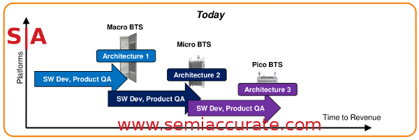
The HetNet problem as LSI sees it
Until recently, you needed very different devices from top to bottom, the hardware on a pico basestation was nothing like that of the vastly larger long distance stations. This mandates some very different software stacks, management tools, and all sorts of other things that bring problems to the poor network trolls running the plumbing 24/7. Heterogeneity is not a good thing here, but there really wasn’t a choice, no hardware was suited for all of the tasks at hand. See what LSI is aiming for now?
Since the Axxia 5500 line can scale from 4 to 32 cores, it can meet all of the demands of basestations large and small. If the pico basestation needs a digitial front end and DSP setup that the big ones don’t, no problem, slap them on. If there are things that the little ones don’t need, pull them out and save die area. LSI hopes to be able to service all of a carrier’s needs from large to small with a single hardware family and the attendant software stack. Carriers like this, it saves them time, money, and headaches, speeds deployment, and makes life easier by simplifying everything. And that is exactly what LSI is aiming for with the Axxia 5500 family.S|A
Charlie Demerjian
Latest posts by Charlie Demerjian (see all)
- What is Qualcomm’s Purwa/X Pro SoC? - Apr 19, 2024
- Intel Announces their NXE: 5000 High NA EUV Tool - Apr 18, 2024
- AMD outs MI300 plans… sort of - Apr 11, 2024
- Qualcomm is planning a lot of Nuvia/X-Elite announcements - Mar 25, 2024
- Why is there an Altera FPGA on QTS Birch Stream boards? - Mar 12, 2024

