![]() Global Foundries has taken a huge step toward mass-market TSVs with their first 20nm wafer with that technology. While it is not a production ready product yet, the wafer is proof that the hard work done up till now paid off.
Global Foundries has taken a huge step toward mass-market TSVs with their first 20nm wafer with that technology. While it is not a production ready product yet, the wafer is proof that the hard work done up till now paid off.
TSVs are nothing new, having been shown off in the lab and on specific single projects for a long time now in various places. Making a single project with TSVs is not exactly easy, but it pales in comparison to the task of offering them as a foundry option that anyone can order. The problem with TSVs as a product is not the tech itself but getting the entire ecosystem moving in the same direction with the same set of design rules. You can watch a technical video about that process here.
There are two types of stacking that TSVs enable, 2.5D aka interposers and 3D aka stacking. While both can be done without TSVs, there are a lot of very compelling benefits to using the technology to stack chips with. On the down side there are a lot of problems too, but since GloFo is offering the tech now those look to be mostly solved.
Power is the most compelling reason for TSV use. With them, you don’t have to ramp voltage up nearly as much to get signals on and off chip. This obviously lowers energy use but can also simplify design by not having as many voltage planes on the SoC. This is closely followed by the ability to quite simply do things that you couldn’t without stacking. The biggest of TSVs is massively wide interconnects at borderline silly ball pitches.
When bonding a chunk of silicon to an organic/fiberglass package (that green thingy under that shiny gray thingy for the non-technical), you can have some issues with thermal expansion. If you are careful it just means your ball/bump pitch needs to be far larger than it otherwise needs to be. If you are not careful there are three things that can happen, one, two, and three. With stacking you bond silicon to silicon and avoid most of the thermal expansion issues that to this day Nvidia management still doesn’t officially understand.
This means you can use much smaller bumps at tighter pitches to put in a very large multiple of the connections in the same space as you could the old way. That changes everything from the design of the SoC to the end device itself. Coupled with the power drop, you can do some pretty impressive things like the 10W Haswell demo at IDF. That was due to Haswell GT3 and Crystalwell, impossible without 2.5D stacking and interposers.
On the down side there are lots of potential headaches. The aforementioned cat herding is the biggest one, you not only have to set standards for customers to follow but you have to set standards that they can afford to follow. It is easy to design standards that are technical marvels which no one can actually afford to buy. Ferraris are not mass market for many reasons but planned scarcity is not the biggest one. Cost is probably the biggest problem in the TSV arena too, closely followed by cost, then cost, and cost.
From there, there are technical challenges like yield. Global Foundries has said that their technology works and yields are not a problem. That said, what exactly are they offering? The technical term is a via-middle process because it etches and fills the via after the Front End Of Line (FEOL) portion of the process and before the Back End Of Line (BEOL) portion. For the non-process minutia oriented this more or less means that you lay down the transistors before you etch the TSVs.
After they are filled in, you then add the metal layers on top like you normally would, and hopefully it all works out. If you haven’t seen a picture of the whole thing, take a look below. The TSV is the massive bit in the center with a 6µm diameter, massive compared to the 10s of nm in the structures on the surface of the device. The transistors can be seen above the S|A logo, the metal layers above the URL. That’s what two orders of magnitude or more looks like in the chip world.
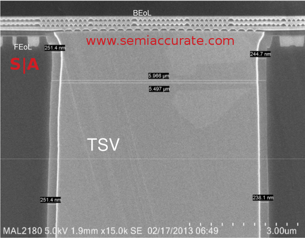
Don’t work for Global Foundries SEM teams if you don’t like mornings
Once you have the TSVs made you can pick a 2.5D interposer structure or a 3D stack for your device. This depends more on chip wattage targeted and cost of the device than anything else. Those two properties more than anything pretty much determine what if any stacking your project will utilize. Why? Technical possibilities followed by cost, cost, and cost.
On the 2.5D side you can pick any interposer size you want up to almost the reticle limit, 32x26mm to be exact. If 832mm isn’t enough for you, IBM can go bigger but not for the same price ballpark, think orders of magnitude more than increments here though. That said, IBM has claimed to be able to do more than 50x50mm interposers, but you had better be making things with Power 7+ margins if you do. That said they are pretty, not to mention pretty active.
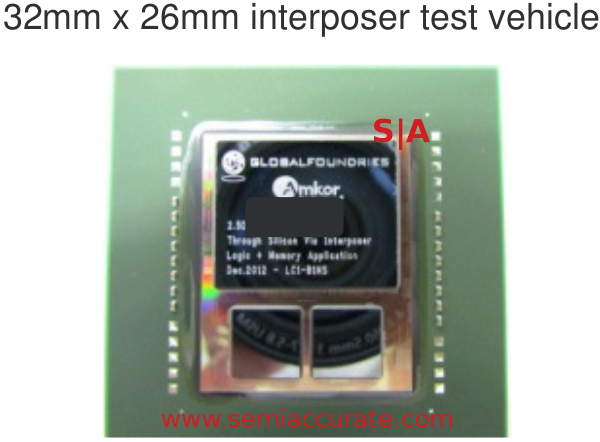
This is what a 2.5D/interposer test vehicle looks like
The GloFo version of the interposers will be made on their 65nm line at Fab 7 in Singapore. From there they are shipped to an OSAT along with the full thickness wafers for backgrinding and assembly. Some foundries are doing it all themselves but GloFo is working with a partner ecosystem, Amkor is mentioned prominently in their presentations but others are right there too. This partner approach has the short-term ‘cat herding’ problem but long-term it provides both standards and options for customers. SemiAccurate feels that the partner approach is the better one long-term, second sourcing means a lot to potential customers.
3D is much the same but without the interposer. Full thickness wafers are sent off to an OSAT for grinding and assembly. If the system works right, the OSAT doesn’t even need to stick with 100% GloFo silicon, good for customers but less so for the fab. Unless GloFo wants to get in to the memory business, setting standards is pretty mandatory and will pay big dividends for them in the long-term.
Both 2.5D and 3D are set for a 20nm introduction, and SemiAccurate is pretty sure that it is going to happen. The singing spring moles of upstate New York (Deepinda snowbancus) tell us that there is at least one 3D project in the process of taping out now and more 2.5D projects imminent. Stacking isn’t a lark at Global Foundries, it is quite real and well past tire kicking stage as we speak. Given how impressive the tire kicking was, full qualification for general use by next year and non-early adopter production in 2015 should bring some amazing device capabilities. Until then, we just get to drool over the tech that makes it all possible.S|A
Charlie Demerjian
Latest posts by Charlie Demerjian (see all)
- AMD outs MI300 plans… sort of - Apr 11, 2024
- Qualcomm is planning a lot of Nuvia/X-Elite announcements - Mar 25, 2024
- Why is there an Altera FPGA on QTS Birch Stream boards? - Mar 12, 2024
- Doogee (Almost) makes the phone we always wanted - Mar 11, 2024
- Intel Birch Stream Boards Speak From The SIde - Mar 6, 2024