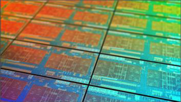
AMD seems to have accidentally outed a rendering of a Summit Ridge wafer at its May 12th shareholders meeting. The image above is an upscaled version of the image taken from the livestream’s slidedeck shown below.S|A
UPDATE 5/22/2016 3:38 PST: Summit Ridge is the high-end desktop (HEDT) product that AMD has previously promised to release in Q4 of this year. It’s expected to be the first chip that integrates AMD upcoming Zen CPU architecture. Expectations are high and Summit Ridge may prove to be a make or break product for AMD.
UPDATE 5/22/2016 3:09 PST: I sent this image around to the usual suspects and I’m hearing some interesting takes on what we’re looking at in this wafershot.
There are clearly two large rectangular structures on each die. All signs point towards these being groupings of four cores and cache. There appears to be a memory interface on the upper left corner of the die.
The arrangement of resources shown here has some interesting implications for AMD’s other Zen-based products namely the upcoming Raven Ridge APU. Raven Ridge is rumored to be a quad core part. Given that Summit Ridge appears to have two quad core modules or groupings and a separate memory interface for each grouping that lines up nicely with expectations of a single module or quad core Raven Ridge. Additionally rumors have also suggested that the Zen-cored server chips that AMD’s working on will range in core count from 16 to 32 cores. These rumors/leaks line up nicely with an architecture that scales by fours.
The question that still remains unanswered is how will AMD scale from this apparently 8 core die to 16 and 32 cores? Will they spring for a larger 16 core die and package them as a multi-chip module (MCM) like with their older Opterons? Or will they utilize some kind of exotic 2.5D packaging technique. Both are interesting, if highly speculative, thoughts to consider.
UPDATE 5/22/2016 3:47 PST: Hans de Vries of chip-architect.com has posted this interpretation of one of the quad core modules in this Summit Ridge dieshot. Suggesting that the somewhat regular looking structures on the edges of the modules are the CPU cores themselves and that there is some form of a shared cache structure present in the center of a module. Again the source image was pulled from a slide on a livestream and then upscaled; thus it’s pretty amazing what kind of information various commentators like Hans have been able to infer about this chip so far.
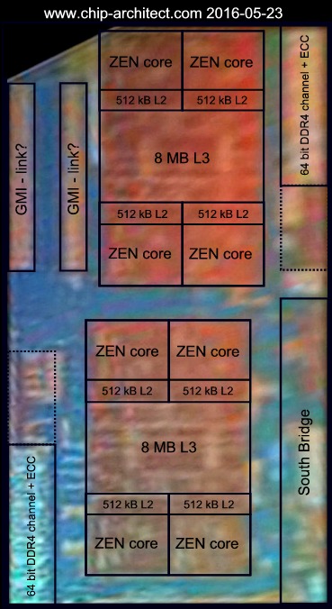
UPDATE 5/22/2016 4:07 PST: Matthias Waldhauer or Dresdenboy of New Citavia Blog has also posted his interpretation of this wafer image. His finding are very similar to what Hans found and the posters in our Forum appear to be leaning towards. Four cores, an L3 cache in the center, and a DDR4 interface on top all appear to part of a single Zen module. There’s definitely more to it than just those macro-level components and there are portions of the die that we can only guess at. It’s worth noting that the cache at the center of the module could feasibly be either an L2 or an L3 cache although most are convinced it’s an L3. Additionally one of the unidentified structures on this chip has to be an integrated south bridge, as AMD promised, if this chip actually is Summit Ridge.
UPDATE 5/22/2016 4:26 PST: JeeBee a regular contributor to our Forums since 2010 has come up with a very detailed interpretation of this Summit Ridge wafer image. Pointing out where he believes the L3, L3 supporting hardware, and L2 caches are located. Most commentators appear to agree at this point on each Zen module housing an 8 MB L3 cache.
UPDATE 5/22/2016 5:06 PST: After more discussion Han de Vries has created another diagram highlighting where we believe the two DDR4 PHYs, South Bridge, and off-chip high-speed interconnect interfaces are. You can compare Hans’ interpretation to a professionally labelled image of AMD’s Carrizo die and make up your own mind. The rather irregular looking area on the top right hand area of the die is probably the South Bridge, as far as anyone can tell. The bottom left hand corner has very regular looking structures leading us to believe that it’s some kind of off-chip interconnect like AMD’s old Hypertransport or a rumored but as of yet publicly unconfirmed interconnect technology called GMI.
GMI has been briefly referenced in patches posted to the Linux kernel’s mailing list by AMD employees. Fudzilla believes that GMI stands for Global Memory Interconnect and that it’s a coherent fabric used for chip to chip communication within the same MCM package capable of up to 100 GB/s using four links.
Thomas Ryan
Latest posts by Thomas Ryan (see all)
- Intel’s Core i7-8700K: A Review - Oct 5, 2017
- Raijintek’s Thetis Window: A Case Review - Sep 28, 2017
- Intel’s Core i9-7980XE: A Review - Sep 25, 2017
- AMD’s Ryzen Pro and Ryzen Threadripper 1900X Come to Market - Aug 31, 2017
- Intel’s Core i9-7900X: A Review - Aug 24, 2017