![]() Samsung wasn’t going to be shown up by IBM at the wafer bragging sweepstakes, so they showed off a 14nm wafer and a 20nm wafer. OK, IBM did it a year ago, but now Samsung has it too.
Samsung wasn’t going to be shown up by IBM at the wafer bragging sweepstakes, so they showed off a 14nm wafer and a 20nm wafer. OK, IBM did it a year ago, but now Samsung has it too.
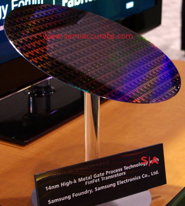
Not much to say here, we showed you the IBM 14nm wafer yesterday, and true to the Common part of Common Platform, Samsung has one too. Yes it is FinFETs, no there were no specs given, and yes it is pretty, and shiny too.
Samsung 14nm wafer
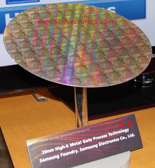
From there, the company also had a 20nm wafer, and no, it is not FinFET based. Some fools are calling the test chips on this wafer Tegras, and that makes me weep for my chosen profession. Why? I showed it to my wife who was a biology major. It took her less than 10 seconds to figure out why it isn’t Tegra, can you? Some ‘journalists’ sure can’t.S|A
Samsung 20nm wafer
Charlie Demerjian
Latest posts by Charlie Demerjian (see all)
- Qualcomm Is Cheating On Their Snapdragon X Elite/Pro Benchmarks - Apr 24, 2024
- What is Qualcomm’s Purwa/X Pro SoC? - Apr 19, 2024
- Intel Announces their NXE: 5000 High NA EUV Tool - Apr 18, 2024
- AMD outs MI300 plans… sort of - Apr 11, 2024
- Qualcomm is planning a lot of Nuvia/X-Elite announcements - Mar 25, 2024

