 At CES, SemiAccurate showed you a dual core Clover Trail phone from Lenovo, now officially called Clover Trail+. This device is about what you would expect, another core, and more everything.
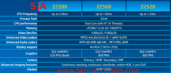
Clovertrail+ launches today, but it has been well telegraphed long in advance, we told you about it over a year ago back when it was just a dual core/dual graphics chip with the cryptic code name “Future“. Now it is Clovertrail+ officially or if that is too hard to remember, there are three official SKUs, the 1.2GHz Z2520, the 1.6GHz Z2560, and the 2GHz Z2580. All have the same silicon, this won’t change until the next gen follow on to “Future”, code named “Next Generation” according to the slides, is released.
Medfield vs Clover Trail+
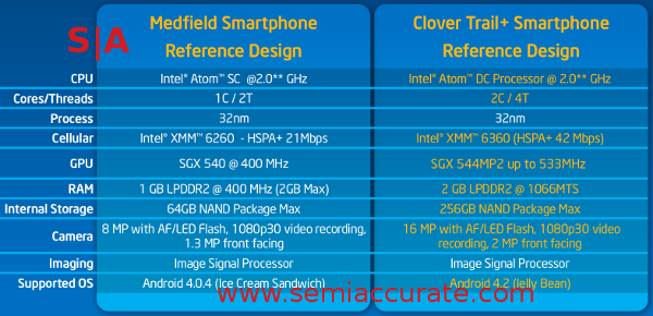
The first question on everyone’s mind is what is the difference between the older single core Medfield and the new Clover Trail+(CT+)? Take a look at our articles on the core and the uncore for a pretty good idea of the tech under the heat spreader. The chart above shows the gross differences, another core for two more threads, double the GPU at 33% higher clocks, twice the RAM at more than twice the speed, two channels of LPDDR2 instead of one, and four times the NAND storage. The camera doubles in size from 8MP to 16MP so the image processor was very likely upgraded, sped up, or both, but no details were given there.
On the software side, the default is now Android 4.2 instead of the older Android 4.0.4 found in the Medfield reference designs. The modem is also seriously beefed up, the new XMM 6360 does 42Mbps HSPA+ twice what the older XMM 6260 could muster. Notice a theme? Twice the cores, twice the GPU, twice the bandwidth, twice the memory, twice the pric… err then it falls apart. Still, it is a nice idea, and twice most everything is not a bad rule of thumb to go by this time. The full lineup looks like this.
Meet the new family
If you just look at the gross specs, it won’t look very different, but there is one very interesting thing not conveyed by those numbers, the non-peak clocks. If you recall, Medfield had three main speed modes, LFM, HFM, and Burst (BFM) with the often quoted 2.0GHz number being peak burst clocks. The reality is that the SoC will spend the majority of it’s life in LFM or below so these clocks are more of a range than a hard stopping point, it can ramp up or down with a lot more granularity than these three points.
With that in mind, LFM goes from 600MHz in Medfield to 800MHz in CT+, HFM steps from 900MHz to 933MHz, and both peak at 2.0GHz, lower in the Z2520 and Z2560. If idle and LFM power didn’t go up significantly, this means the new parts are a bit more efficient clock for clock than the old, but given how much time is spent at idle, it is probably hard to detect with an external meter. Still, it looks like progress.
We could bore you to tears with the benchmarks, but lets just say that if your app is threaded decently, it should get a good kick in the bottom line from CT+. The peak speed didn’t go up much, but memory bandwidth increases almost 5x likely to support the more than doubling of GPU resources. Medfield was not exactly a slouch in performance, but the graphics were not enough to set the world on fire. That seems to have changed, and with the memory bandwidth available now it should really shine. If for no other reason, memory should differentiate it from the other SoCs with the same Imagination GPU resources.
Another thing that Intel was sadly only talking about in terms of features, not the underlying hardware, are some of the advanced imaging capabilities. At CES, Nvidia was crowing about their advanced imaging capabilities in Tegra 4, no ‘i’. SemiAccurate was unimpressed mainly because it is a feature that all the next gen SoCs have, Nvidia was just the first to shout about it. Most others, CT+ notwithstanding, have the HDR features of Tegra 4 and a whole lot more. We expect all new higher end SoCs from this point on to have most of these features, most likely because the carriers are demanding these as checkbox items.
This isn’t to say Intel is not doing things well, they most definitely are. They have a few features in addition to the one-click HDR functions that could be very useful. One is called Zero Shutter Lag (ZSL) and the other called Perfect Shot. The idea behind both is the same, if your camera doesn’t have to wait between frames for image processing, you can just keep taking pictures as fast as you want, effectively a movie made from full still frames. Take them and put the result in a ring buffer instead of saving it all out to storage, and you have the basis for both technologies.
When you press the shutter, the ZSL mode will effectively pause the image capture, but not until after it takes a few more frames. The shutter click becomes the mid-point in the capture stream, and everything for a few tenths of a second before and after is grabbed as well. This gives you several very similar pictures to choose from after the fact. ZSL lets you go forward or back in time after the shutter is pressed so if you missed the ‘perfect moment’ in time, you can just rewind or fast forward later. You then pick the frame you want from the stream, then lie to your friends about your ‘mad skilz yo’. [Editor’s note: Intel designed this feature as a response to Charlie’s photo-taking skills.]
Perfect shot is a similar feature, you can take a picture of a crowd or a group of people and like ZSL, it takes a stream of shots. The slightly worrying part is that it automatically looks for faces with face detection, picks the best one, and merges the images to effectively make a single frame with no one blinking, frowning, or whatnot. This could be handy, but I can see problems when algorithms try to estimate human emotional responses. In addition, the face detection software seems really broken, take a look at the image below, this is _NOT_ me or anything even close to what I look like. Wait for V2.0 on this tech.
It didn’t recognize the author, not sure who this guy is though
Last up are the details of the chip itself. All we can say for sure is that the package is 14x14mm, up from 12x12mm. No die sizes were given this time, and Intel didn’t even release a die or package shot, just a BS rendering to obscure details. What they don’t realize is that any decent competitive intelligence team had samples weeks ago, nothing relevant is being protected at this point. That said, the PoP construction is the same as Medfield, if you are not familiar with it take a look here, it is really nice.
Overall, Clover Trail+ is not a massive step forward in features, it mainly takes the old Moore’s Law approach of twice everything for about the same power use. It enables a bunch of additional features like ZSL by simply providing the raw horsepower to get it done. Real world power draw should go down too if the added cores can keep the time spent at higher clocks down too, same for the added GPU units. In essence just it is more of everything, but you don’t see much of that in the peak numbers. What you get is less dips in performance, better battery life, but no big high points to shout about. It is a solid evolution of what Intel had last year, and that is not at all a bad thing at all.S|A
Charlie Demerjian
Latest posts by Charlie Demerjian (see all)
- What is Qualcomm’s Purwa/X Pro SoC? - Apr 19, 2024
- Intel Announces their NXE: 5000 High NA EUV Tool - Apr 18, 2024
- AMD outs MI300 plans… sort of - Apr 11, 2024
- Qualcomm is planning a lot of Nuvia/X-Elite announcements - Mar 25, 2024
- Why is there an Altera FPGA on QTS Birch Stream boards? - Mar 12, 2024


