 We told you about the Intel Xeon E7 v2 line earlier, now lets take a technical look at these chips. We will focus on the big die part, 15 cores, three rings, and a lot of cache.
The first thing you may think of when looking at the Ivy Bridge-EX die is how much it looks like the Ivy Bridge-EP line of chips. The two look so similar because in large part the Ivy-EX CPU is lifted from the Ivy-EP design and so inherits all of the features from that device. This is a massive advance from the 2011 era Westmere-EX line, the last series of 4S+ chips Intel released. The chip looks like this.
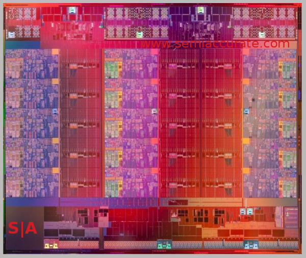
A big die for a big chip
As with Sandy and Ivy Bridge chips, the Ivy-EX die is based on a familiar ring structure with each of the 15 cores associated with an L3 cache. For the largest models, each slice has 2.5MB of cache associated with it but there are other dies with only 2MB per slice. If you fuse off a core you also fuse off the cache that goes with it so cache size is core count times 2 or 2.5. If you want the details, we wrote them up here.
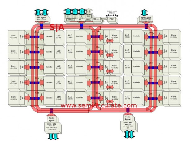
With one exception this could be Ivy-EP
Cores are arranged into three columns of five with three rings each connected to two columns. In previous versions of Sandy and Ivy with 10 or less cores, there were only two rings and both connected to all cores but ran in different directions. Once you get to the 12 or 15 core models, the ring count goes to three but each core is only connected to two rings. This allows each core to connect to every other core on a ring but unlike the 10 core versions that connection is not bi-directional. In practice this will likely have little effect on average cache latencies, but technically speaking it is inferior.
At this point the Ivy-EX is exactly the same as the largest Ivy-EP, so what differentiates the two? Both still have two Home Agents supporting four channels of DDR3-1600 plus a generalized IO block with up to 32 PCIe3 lanes, so thus far they are identical other than PCIe lane count. On a macro level the answer is a second QPI agent connected to the rings which allow for scaling beyond two sockets.
Each QPI agent supports two QPI links which is why EP scales to two sockets directly connected or four sockets with a two hop maximum. By adding a second QPI agent, Intel ups the socket count to four for directly connected CPUs or eight glueless but indirectly connected sockets. One thing to note is that the second QPI agent only has one lane active, the other has two so Ivy only has three active QPI links. Another lane would mean less hops on the 8S configuration but many more pins, cost, and headaches for the rest. It all looks like this.
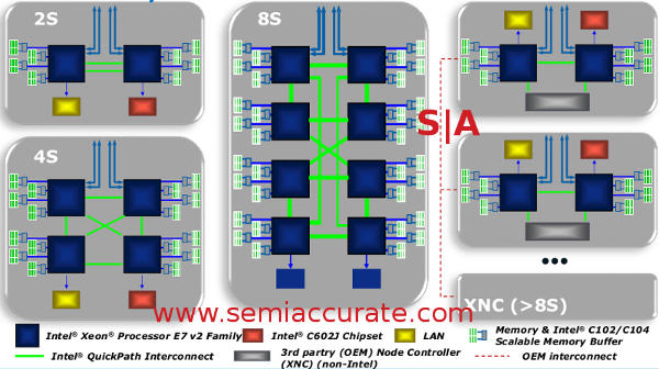
Note the 4S configuration, EP can’t do that
With all the added slices of cores and caches, the bandwidth on die goes up dramatically to a claimed 450GBps for L3 access across all cores. More interesting is that with the high core count and three-ring structure, the average cache access time is only 15.5ns. This is quite remarkable considering each L3 line is hashed and saved in a slice not necessarily associated with the core that used the line.
Moving data between sockets presents a problem as clock speeds rise, the faster you are the more painful an off-die request becomes. One method of dealing with this is the new QPI V1.1 link that runs at 8GT/s instead of the 5GT/s of the older versions. If these numbers sound like they are based off of PCIe, that is about right, QPI is based on PCIe with a heavily patented overlays. That said the higher speeds do take a big chunk out of latencies, 290ns on Ivy-EX vs 395ns on Westmere-EX, even if route-through times are similar.
Speeding up off die transmissions is nice but avoiding them is a much better idea. To address this issue, Ivy-EX has a new home snoop protocol which updates the source snoop of Westmere-EX. Home snoop starts with a home issued snoop protocol, hence the name, and supplements that with an in-memory directory. This directory is expanded to two bits per line so three states, Invalid, Shared and Any, can be supported. This greatly reduces unneeded snoops and Intel claims it works very well for non-fully connected systems like the 8S 8800 line.
Ivy-EX can still do opportunistic snoops and the levels to do so are are dynamic and based on workload behaviors. In short if the system sees there is extra bandwidth available and recent behaviors indicate it is warranted, it will issue snoops in an opportunistic manner. These thresholds for local, remote, and other can be set in the BIOS and the system is capable of adapting from there. In addition there are many other snoop optimizations involving caching agents, IO, and anything else Intel could squeeze a gain from. The higher the socket counts, the more important coherency becomes, and Intel has gone to great lengths to optimize things on that front.
As we mentioned earlier there are two home agents in Ivy-EX just like Ivy-EP but they are slightly different. Ivy-EX does not connect to DIMMs directly, it has a link called SMI that connects it to a memory buffer. Before we get to that, the home agent itself has been dramatically beefed up to support the greater needs of the system. Most notably the buffering has been increased to support up to 240 transactions in flight for each socket, that would be 120 per home agent. On top of this the buffers for the memory controller itself have been enlarged and it has much larger transaction queues too.
The interesting part starts with the two SMI links per home agent, and each connects one of the two memory controllers per home agent to a memory buffer code-named Jordan Creek (JC). Each JC can have two channels of DDR3, DDR3L, or LR-DIMMs, registered and buffered of course, with three DIMMs per channel. That means six DIMMs per JC, four JCs per socket, or a total of 24 DIMMs per Ivy-EX. Since 64GB DIMMs are supported that means a maximum of 1.5TB of memory per socket. Specs however don’t tell the story here though, the good stuff is in the details.
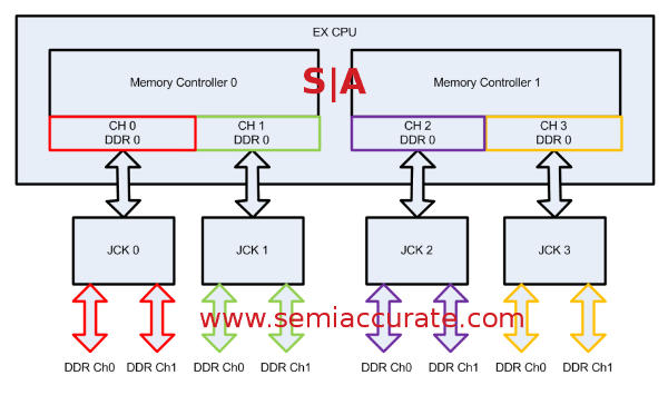
E7 memory with Jordan Creeks in Lockstep mode
Since the Jordan Creek buffers connect to the memory controller in the home agent via an SMI2 link, it is not constrained to DDR3 frequencies. Intel takes advantage of this with two modes, one is called Lockstep Mode (LM), the other Performance Mode (PM). In LM the SMI2 link is driven at DDR3 speeds, 1600MHz at the high-end. Each JC has two channels of DDR3-1600 and talks to the memory controller across a SMI2 link also running at 1600MHz. Since this link is the width of a DDR3 DIMM, 64-bits, you can see it is a bottleneck. In Lockstep mode the JC is effectively seen as one 128-bit wide channel of DDR3
If the SMI2 link is a bottleneck, why would you want to do things like Intel does? LM allows Ivy-EX to do some fancy error correction that they call DDDC or Double Device Data Correction, a form of RAS that allows a machine to map out up to two failed DRAM die. With the older SECDED a system could detect two-bit errors but only correct things in the case of one. DDDC allows the controller to correct both, it is a much more advanced ECC scheme in effect.
Update Feb 19, 2014 @ 1:00PM: Intel says the SMI2 link is not a bottleneck in Lockstep Mode, it is just slower.
The Lockstep part of Lockstep Mode allows Intel to see a wider DIMM and use that to detect and correct errors. It takes a bit of time and costs memory performance but it is no worse off than an Ivy-EP. You are trading a bit of performance for reliability, something most customers of the big E7 systems are more than happy to do. With thousands of users and millions of dollars per hour of potential downtime costs, this is a good trade.
That brings us to Performance Mode and as the name suggests it is a lot higher performance. Instead of a 1600MHz SMI2 connection, performance mode ups speed to 2667MHz and sees the JC as two 64-bit wide channels. This forces the maximum DRAM speed down to DDR3-1333 but allows the controller to see both channels at full speed duplexed across the narrower but faster SMI2 link. In effect it almost doubles DRAM bandwidth but makes latency slightly worse. The only problem is that you lose DDDC hence the performance side of the performance or reliability trade-off.
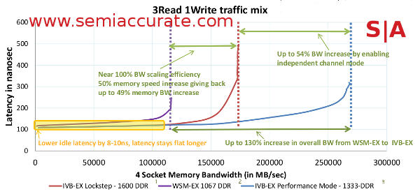
The two modes do make a big difference in performance
How well does PM do vs LM? Intel showed us the handy graph above that compared the two to the previous Westmere-EX line which supported up to DDR3-1067. With 50% more memory bandwidth, LM ends up with 49% better memory performance also known as damn good scaling efficiency. In PM however things are vastly better with performance 54% higher than LM and 130% higher than Westmere-EX even though the memory is only a net 33% faster. Not bad at all, and better yet you can pick which mode you want to use for your particular problem, reliability or performance.S|A
Update Feb 19, 2014 @ 1:00PM: Replaced System diagram picture with corrected one from Intel, corrected PCIe lane count to 32 from 40. Also clarified the DDDC explanation to point out that it maps out bad chips rather than corrects the error on the fly ala ECC.
Have you signed up for our newsletter yet?
Did you know that you can access all our past subscription-only articles with a simple Student Membership for 100 USD per year? If you want in-depth analysis and exclusive exclusives, we don’t make the news, we just report it so there is no guarantee when exclusives are added to the Professional level but that’s where you’ll find the deep dive analysis.
Charlie Demerjian
Latest posts by Charlie Demerjian (see all)
- What is Qualcomm’s Purwa/X Pro SoC? - Apr 19, 2024
- Intel Announces their NXE: 5000 High NA EUV Tool - Apr 18, 2024
- AMD outs MI300 plans… sort of - Apr 11, 2024
- Qualcomm is planning a lot of Nuvia/X-Elite announcements - Mar 25, 2024
- Why is there an Altera FPGA on QTS Birch Stream boards? - Mar 12, 2024