
![]() Samsung was showing off their 20nm/14nm hybrid process wafers at Common Platform, the first one SemiAccurate has seen in the flesh. We won’t go in to the details of the process itself for now, but lets just call it 14nm for simplicity.
Samsung was showing off their 20nm/14nm hybrid process wafers at Common Platform, the first one SemiAccurate has seen in the flesh. We won’t go in to the details of the process itself for now, but lets just call it 14nm for simplicity.
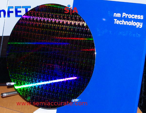
Samsung 14nm test wafer
We will go in to a bit more detail about the process itself, or at least the GloFo version of it later, lets just say it is a 14nm transistor with 20nm everything else. GloFo calls it 14xm, Samsung was still setting up the booth when we took pictures, it isn’t really called “nm Process Technology”. In any case, this hybrid process is real enough at Samsung; IBM and Glofo are likely there or really close too. Since Samsung was the only one to display their toys publicly though, they get the credit this time.S|A