![]() Last week ARM unveiled their new IP that will be featured in the devices consumers buy in 2025. SemiAccurate took a long look at the offerings and likes what they see.
Last week ARM unveiled their new IP that will be featured in the devices consumers buy in 2025. SemiAccurate took a long look at the offerings and likes what they see.
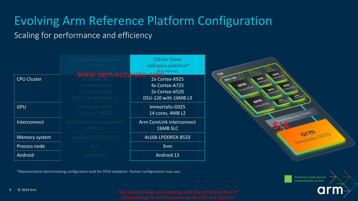
The headline news is the new naming which may sound deep but it is basically the same old same old with a new coat of paint. What was TCS is now CSS! Yes, Total Compute Solution is now Compute SubSystems for Client. What’s the difference? The name really but the changes from the 2023 layout to the 2024 layout are quite significant. How significant? 10 cores, 14 GPU cores, big caches, and more.
TCS is Now CSS
Lets start out with the new cores, the Cortex-X925 is the obvious successor to the X4 because X5 is far too obvious and Blackhawk is just a cool code name. Cortex-A725 is a mildly tarted up A720 and the A520 is, umm, on a new 3nm node now. Actually all of CSS is implemented on TSMC 3nm in 2024. The DSU-120 now has 16MB of L3 which should pay some significant power and performance dividends if it is fully implemented as will the CoreLink interconnect with a similar 16MB of system cache.
Just looking at the spec list for CSS you can see the ‘recommended’ device for high end phones and the like is a 10 core SoC with 14 GPU cores but this time around things go from one to two biggerer cores, and yes we meant that misspelling. This is a pretty direct indication of where ARM sees the market going and we agree. That said three tiers of cores is a bit silly but it will likely take a few more years for them to come fully around to sanity. All three tiers support the V9.2 architecture as you would expect.
On the GPU side, a ‘mere’ 14 cores are recommended this year which is well within the scope of last years GPU structures. If that is too limiting, you can go up to 24 cores this time around, a 50% increase from the previous cap of 16. Likewise caches are up here too but more on that when we look closer at the architecture. So overall, bigger everything, more of everything, and moving up the ladder on everything too. Except Android which is officially still 13.
The Cores:
On the core front we will start off with the low end, the A520 ‘small’ core. Imagine taking the A520 from TCS23 and shrinking it to 3nm while cleaning up a little low hanging fruit for a claimed 15% energy savings. On the performance side the new A520… did we mention the power savings? Yes we did. Oh look, there is a big core over there.
So you want to know about the A725, the spiritual and actual successor to the A720. This new version can have up to 16MB of L3 per DSU cluster and up to 1MB of L2 per core. Given that caches are the one thing that almost every ARM partner tweaks, expect to see variants all over the map on these two specs.
Officially ARM nearly lost the plot with the A725 overview by starting it out with “Targeting AI/gaming use cases”. SIGH, make this plague go away. Otherwise the goals seem sane but, enough with the AI everything! Not because of AI the shrink to 3nm and the obligatory clean up from the A720 means you can have 2x the L2, 1MB now, with the same area as before. That is the most obvious change for the mid-core but there is an area optimized version if you need more. Or less. Or, well you understand, just pick the physical implementation that most fits your needs.
The list of updates is short and fairly low level but they do add up. The register file structures were enhanced, the re-order buffer is bigger, and the instruction queues are longer. As you might guess the cache enhancements feed into this, again pun intended, so the A725 should be able to make good use of the updates. None of these tweaks are visible from a high level overview so there was no block diagram this time around.
All in all if you take the highest performance version of the A725, ARM claims a 35% “performance efficiency” improvement over the A720. Since the power efficiency is a claimed 25% better, well, performance isn’t up all that much. The other stat ARM gave out is a 20% improvement in L3 traffic which should be more than enough to feed the deeper structures. All in all the A725 is a mild enough tweak to not justify a full rebranding but the gains appear real enough. For AI obviously. Sorry, the urge to mock is too strong.
Biggerer Is Betterer:
That brings us to the biggerer core, the new X925 CPU that is no longer X5 or Blackhawk either. This one does have a lot of updates, and we mean a lot, but not enough to justify a new block diagram. Pity that but it is a good part nonetheless. Luckily for us the design goals for the X925 did not include AI but do include “think bold” which ARM seems to have done with a claimed cutting edge architecture. Given the trends that everyone is moving towards in CPU design, ARM seems to be right on target with this one.
X925 is Clearly 921 Better Than X4
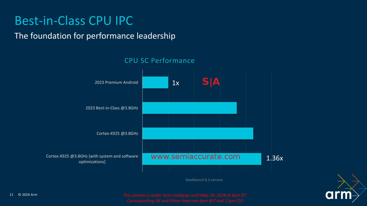
As you can see the performance at 3.8GHz, the claimed peak clock for the X925, is a bit over 30% higher than the older X920, err X4 core. Even the most juiced X4 trails Blackhawk by the high single digits, 10% if you use all the software tweaks. In any case the X- cores are tuned for peak performance and that is what the X925 delivers. A claimed 14% increase in application launch speed will be welcome as will mid-teen percentage improvements in benchmarks. AI performance is up by about double that number and since ARM did not overplay AI we won’t mock it. In any case the gains appear solid, more than the usual minor gains that often accompany a new core.
So how did they do it? Again lots of minor changes rather than any huge reworking but it all adds up. The front end is where it all starts and ARM upped the instruction window by 2x, quite the jump. Add in more conditional branch bandwidth to support higher accuracy and you have a hair fewer mispredicts. Given how low the rate is now, on the order of low single digits per 1000 instructions, a small gain pays big dividends here. Remember that each mispredict has a huge latency penalty so the gains here are worth it.
Similarly the fetch improvements start with doubling the L1 I$ bandwidth and doubling the L1 iTLB as well. This is aided by earlier fold out of unconditional direct branches, basically everything gets better and the results are fed faster so the front end stalls quite a it less often. Both the branch prediction and fetch improvements do miss at times and the 3MB L3 and bandwidth gains help a lot when things don’t go as, err, predicted.
On the core side, ARM claims the X925 is the “Widest, highest-throughput microarchitecture in the the industry”. This claim will lead to emails pointing to some corner case that disproves the claim but, well, send them! That said it is likely the case even if it is academic, net performance matters in the end, not a single spec, even if it is cool.
X925 is More of Nearly Everything
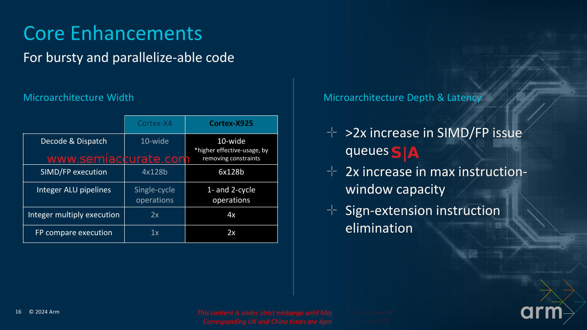
As you can see from the chart above, the X925 is a tad ‘more’ than the X4 it replaces but some bits need explaining. The 10-wide decode and dispatch is more effective because a lot of things that were not allowed previously are now allowed, hence the removal of constraints bit above. This new found basically means more instructions are dispatched per cycle even if the width doesn’t grow. Those instructions are stored in much longer issue queues when dispatched, 2x for FP/SIMD and more for everything else.
Luckily the resources to crunch these instructions have grown too, 50% more SIMD ops per cycle, 2x the FP compare rate, and 2x INT multiply rate. All of this is useful for, shudder, AI but also everything else. In any case it goes a long way to explaining why a 15%+ benchmark improvement is paired to a 30%+ AI compute gain. Throw in a 2x ROB boost, 1500 instructions now, and you have a beast of an execution machine, as claimed. ARM says the efficiency improves too so, well, the X925 looks good so far.
The back end was also improved, most notably because there are no claims about AI here even if the changes do help that workload. That said there are is now one more load pipe for a total of four and the L1 D$ bandwidth doubles. Why? Remember that SIMD increase and all those FP gains? You have to feed them and the L1 is what they read from.
The other changes are a bit less dramatic but still quite useful. OoO depth grows 25-40%, store-to-load forwarding is improved, and data prefetcher improvements are ‘generational’. That said shaving a few cycles off latency here and there does a lot to keep things moving, especially the often dreaded store-to-load time.
As you can probably tell the overall architectural goals of the X925 are ‘more’, and they hit those marks. The core can do a lot more per cycle, ARM claims IPC leadership, and more importantly can keep things fed. Larger caches are the starting point but wider everything, higher bandwidths, and deeper queues all keep things from stalling or bottlenecking. If the claimed numbers survive the translation to real world devices, it looks like ARM is on to a good thing with the X925.
Uncore Is Improved Too:
Cores are all good but if you can’t tie them together with the rest of the system well it is all for naught. ARM didn’t neglect the uncore with the new DSU-120 but the changes are a bit less dramatic. The cluster size is for the 2024 DSU-120 is still 14 cores, and they can support 14 big cores without cheating by putting paired A520s on a single port. There is a reference design with 12 X925s and 2 A725s so we are getting closer to the two tier sanity point after all. In any case the high level view for the DSU hasn’t changed much but the details have.
As you might guess the big improvements are power savings and more throughput, both are needed to support the higher performance devices you place on it. The claim is 50% typical workload power reduction and 60% lower cache miss power. Much of this comes from optimizations but the biggest savings come from cache granularity and sleep changes. This is actually more exciting than it sounds, cool even. No that wasn’t meant to be a power pun even if it was.
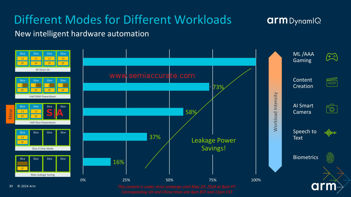
The New Cache Powerdown Options
The blue bars represent the savings from the ability to power down L3 cache slices partially or entirely. With the new DSU-120, ARM added a bit more granularity to the options so instead of all or minimum active slices, you can now have a half awake cache to match the typical user state. This does exactly what it sounds like, you clear the caches out at low loads and power down the slices as needed, off leaks less than not off. With that stunning revelation we will point out that leakage matters a lot for standby and other mobile uses that phones are known for, don’t discount this change.
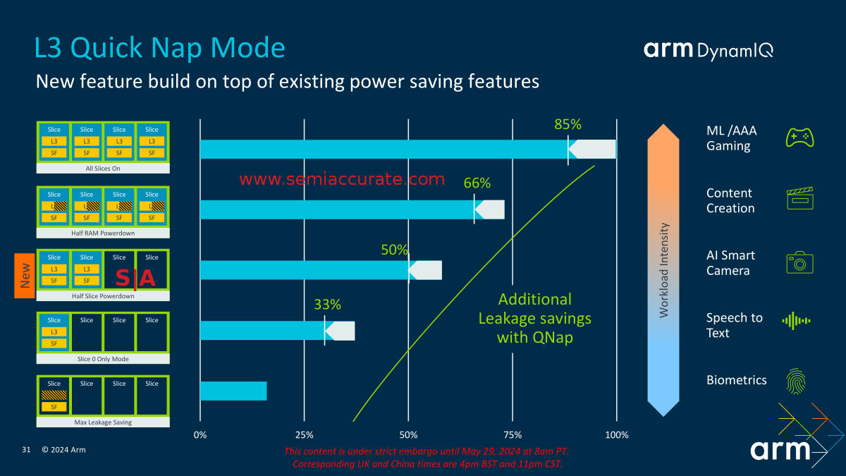
Quick Nap is What it Sounds Like
But wait, there’s more! Introducing L3 Quick Nap Mode which does, well, exactly what it sounds like and puts the caches to sleep faster and deeper than before. Quick Nap shaves a few percentage points off power use but does it more often than before so the gain in the real world is substantial. Think of it as turning the dial down a bit before you need to take the drastic step of saving the data out and powering down the slice, the quick part in the name is the giveaway.
If you look at the added consumption rates for the big cores, the increased ‘typical’ count for them, and the bandwidth heavy new use cases they will face, fabric efficiency is a big deal. Big caches help but the data still needs to be moved in and out, and more of it is flung around at greater speeds than before. The updated DSU-120 will help a lot but you will probably never see the results directly in any benchmark.
GPU Time:
Lets look at the new ARM GPU lineup for CSS with three new cores, Immortalis-G925 on top, Mali-G725 in the middle, and Mali-G625 at the bottom. Actually there is only one new GPU core, the distinctions are simply count and features but lets pretend there are really three new devices to not hurt the feeling of ARM personnel. Just smile and nod if they ask, it works. I am going to get texts for that crack, I just know it.
On an overview level, the cap has been raised from the previous 16 cores to 24 this time around. On the CSS recommended configuration, ARM ‘only’ recommends 14 cores but if you want to blow a hole in your silicon budget, more is there for the taking. In any case to get the Immortalis brand you need to have at least 10 cores and ray tracing. Since the branding has moved from G720 to G925, how can you resist, it is 205 G’s better! If you have between 6-9 cores you can use the Mali-G725 sticker and 1-5 cores will sport the Mali-G625 brand. Ray tracing hardware is optional on all the lesser Malis should you need it and of course cache sizes are configurable too.
Core count is a brute force improvement but there are lots of architectural changes as well. ARM claims high 30% numbers for performance in compute applications, 30% power savings, and 52% improvement in heavy ray tracing workloads. These are all for a 14C G925 vs a 12C G720, 14/12=1.167, but the power savings point to the gains being quite real.
Fragmenting Benchmarks And Rays:
Sounds Simple But Hard To Do
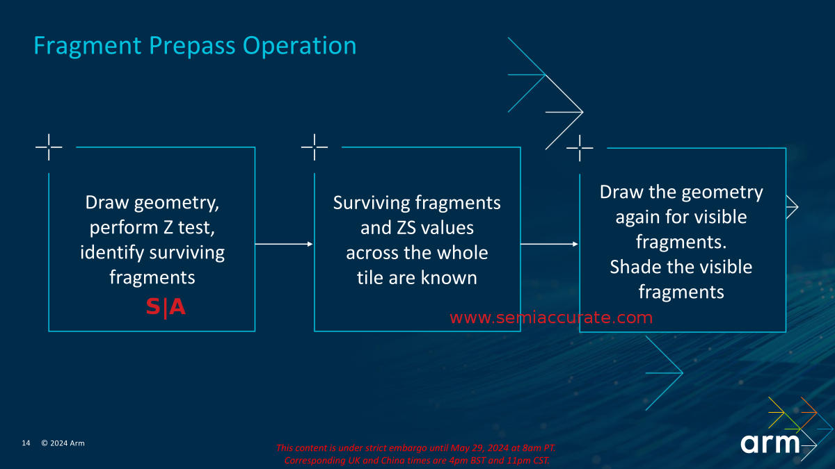
One of the biggest gains comes from Fragment Prepass which ARM says saves up to 43% of CPU cycles on a render thread. It works by culling more fragments earlier and faster so the work in later stages of the pipe can be avoided. As you can see above the idea is pretty straightforward if all the fragments are opaque. The GPU does a Z test, figures out what is visible and throws the rest away as early as possible. That test means the depths are known up front so when the GPU redraws the scene/tile, it only has to draw and shade the visible ones. In short it does a quick pass to determine what work doesn’t need to be done and calculate some values up front, then a full render pass with everything pre-culled and some bits pre-calculated.
This means the objects don’t need to be sorted and work that isn’t seen isn’t done, something that can be said about nearly every GPU improvement for the past decade or three. Fragment Prepass does what it sounds like and does an early pass to cull as much as it can before the heavy work needs to be done. It may sound a bit duplicative but it works quite well and is compatible with all the current efficiency improvements.
On the ray tracing side ARM improved things this time around to the tune of 27% more performance with a hair less memory traffic too. The interesting bit is that ARM allows the coder to trade off accuracy for speed to the tune on a claimed 52% better performance and 57% less memory traffic. Since the developer knows what visuals matter and when they are needed, this could pay dividends if used judiciously. The memory part is the intriguing bit, ray tracing is basically a scatter/gather nightmare that reaps huge rewards when minimized.
But Wait, There’s More:
There are a lot of other interesting bits to improve efficiency on the new GPUs. The most interesting in our eyes is the ability of the Tiler to fuse geometry. A triangle has three points that need to be computed and two triangles have six points, we understand that this is complex math but bear with us. If two triangles share a edge as they likely do on any surface, the tiler can ‘fuse’ them into one unit that has four points. This means a 50% reduction in computation when placing the result in space, a non-trivial reduction.
On the compute front end there are a bunch of new instructions to work with. More things from higher level APIs that needed to be emulated can now be executed directly as a single command. This saves quite a bit of time even if those commands are not seen very often. These instructions probably have some power benefits even if they are not explicitly called out by ARM.
There are a few more minor changes that again all add up. 2MB pages are now supported, the tesselation units are doubled to now match the FMA unit count, and the Z Stencil unit is gets more features and performance. Unless you write some low level code for game engines, you will probably never notice these updates but the results are solid enough.
All in all the new GPU range is pretty decent. The new scaling to 24 cores is unlikely to be see in real world silicon but the headroom is there if you need it. Efficiency changes will be felt by almost every user, gaming is one of the heaviest power draws so small gains have outsized effects. This all assumes the developers take advantage of the changes but they are usually pretty good about adopting new tech.
What Does It Mean:
All of these changes are interesting but the most important is probably ARM’s increased offerings of CPU and GPU physical designs. This time around TSMC 3nm is the target but if Intel’s Foundry conference attendance and speaker list was any indication, don’t be surprised to see Intel 3/18a implementations too. *COUGH*. No clue who though, really. :)
In the end the new ARM CSS is bigger, smaller, faster, more efficient, and more complex. Three tiered cores are still silly but the move to more larger bits on the reference design is a solid if obvious move. The X class cores are significantly improved this time around, 921 better than last year, and the lesser cores get some tweaks here and there. The GPUs get a big kick to scalability, performance, and efficiency and the interconnects tie it all together better too. CSS may not be as radical a change as TCS23 but it still has solid gains. Now we just have to wait half a year to see the result in customer silicon.S|A
Charlie Demerjian
Latest posts by Charlie Demerjian (see all)
- Qualcomm AI/Copilot PCs don’t live up to the hype - Jun 18, 2024
- ARM Outs Their New IP lineup for 2024 - Jun 11, 2024
- Microsoft Throws Qualcomm Under The Bus Too - May 10, 2024
- Microsoft Absolutely Screws Intel and AMD Over AI PCs - May 8, 2024
- Qualcomm Is Cheating On Their Snapdragon X Elite/Pro Benchmarks - Apr 24, 2024