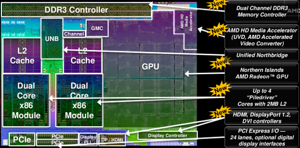
 Part 1 of the series on Trinity covered the core itself, and the changes from Bulldozer to Piledriver. Part 2 takes a look at some of the surrounding pieces of the chip, mainly the interconnects and uncore.
From core to uncore – The UNB and SRQ:
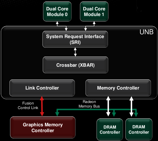
Moving out a step, we get to the Unfied North Bridge (UNB). In many ways, this is the heart of the beast, but not quite as, umm, whole-heartedly as it was in Bulldozer. If you recall, the System Request Queue (SRQ) is a a massive and somewhat intelligent traffic cop that sits in front of the cores. It is the brains of the Unified North Bridge (UNB), AMD terminology for pulling the memory controller and a lot of the I/O on board the CPU while adding intelligence via the SRQ to the mix.
Trinity UNB and attached parts
Llano was the last AMD chip without a UNB, and the difference between it and Bulldozer may appear somewhat pedantic, but the new way is technically speaking, a massive step forward. Llano had a simple bus between the CPUs, GPUs, and memory controller. That is a misnomer, Llano had a lot of busses, and busses are dumb. Dumb interconnects are not what you want for cohesion, and Trinity needed to be a cohesive whole.
With the UNB’s intelligence to this mix, instead of shoving things out on to the bus, busses, crossbars, or whatever, the SRQ can prioritize, optimize, and make things run a lot smoother. If low priority traffic is in high volume, the SRQ may pause them for critical things like interrupts and snoop traffic. The UNB allowed Bulldozer to do a lot more between the cores, memory, and hypertransport connected miscellanea.
If you move on to the UNB in Trinity, it adds one thing that is not in the Bulldozer UNB, a box called Link Controller (LC). This LC is critical for Trinity, and all future Fusion chips. What it does is put a direct path between the GPU memory controller and the CPU Memory Controller(MC). We will cover this later in the article, but GPU memory requests in Trinity are all routed through the CPU memory controller, and then out to main memory where applicable.
Adding the LC to the UNB allows all memory spaces in the system to be mapped to a single flat space. All the tricks that were put in place for memory mapping, virtualizing memory, hard separation of memory spaces between processes, and address translation are now applicable to the GPU as well. It isn’t totally seamless, the CPU MC is separate from the GPU MC, but since one is routed through the other, it just takes a simple add or subtract to map it all to the same space.
For GPGPU workloads, this is a baby step, the killer of latency is still present. For everything else, it is functionally indistinguishable from a single MC for the entire system. Better yet, to the non-AMD driver writer, it is functionally the equivalent to a completely unified memory space and single MC, GPGPU software writing nirvana. You can see where AMD is going to go in Kaveri, or possibly the generation after that, and it is a good thing.
Back to the UNB and SRQ, these two allow Trinity to put smarts behind routing data to and from all the CPU’s components, and do it from a single source. If you want to prioritize GPU traffic, no problem. CPU traffic? No problem. I/O, same. What will be exposed to the end user, or even to the OS/driver writer in this generation remains to be seen, but the pieces are there to do what everyone has been crying out for since the last century, seamless unification of CPU and GPU.
As a speculative aside, the FPU in Bulldozer and Piledriver is connected to the INT cores as a co-processor, with one FP shared by two INT units. Think about that with respect to future Fusion SoCs, especially in light of the UNB, SRQ, LC, and MC’s. This is how AMD is likely to truly integrate GPUs in to the CPU when the time is right, something that is likely well underway by now.
As you can see, the UNB has three types of inputs, the CPU modules, the GPU, and memory. That is why it forms the heart of the Fusion architecture, it manages basically everything. Future performance advances will happen here, it doesn’t take a huge leap of logic to add a local memory cache ala Haswell/Crystalwell or Tiran (before the roadmap reshuffle). This is how the future will happen.
Un-un-core – The rest of the pieces:
The other main pieces connected to the UNB, those are the GPU MC, the Fusion Control Link (FCL), and the Radeon Memory Bus (RMB). This looks very much like Llano’s simplified architecture with Onion and Garlic, aka the last generation FCL and RMB. They are now getting massive upgrades with the FCL now at 128b wide and the RMB is 256b, each bi-directional. This means that the GPU has complete and full bandwidth access to cache, system memory, and the UNB, but still respects the SRQ’s orders.
The block diagram that matters
More importantly, the GPU memory controller talks to physical memory like an x86 CPU does. This generally means backwards, broken, and wholly stupid, but it is far easier to change an integrated GPU’s MC than the entire x86 world, hardware and software. Technically, it is a step backwards for a GPU MC, but totally transparent to those other than the once sane AMD GPU MC designers, may they someday find peace after this indignity. That said, the end result is what allows a single memory space to happen, and the blasted sanity of a few MC designers was deemed an acceptable loss. Sorry guys, it really was worth it.
This means that, latency aside, the GPU is no longer a second class citizen in the CPU world. If you recall from last year’s AFDS conference, AMD’s Phil Rogers laid out a roadmap for Fusion integration. At the time we were a little past column two, but not yet at column three. The big stumbling blocks were unified and coherent CPU and GPU memory spaces, plus other related items. Guess what Trinity brings?
Column four, basically the ability to seamlessly pass threads between the CPU and GPU, require, wait for it, a single memory controller for both the CPU and CPU. This will drop latency, and allow what Trinity can do to be done in a sane time frame. The last few columns happened at a yearly cadence, so guess what Kaveri is likely to bring to the table? No points for this one though, I just gave it to you. That is what will allow FSAIL/FSA, now called HSA, and pave the way for AMD and ARM CPU Frankenstein experiments.
Once again, RBS ‘analyst’ (Note: For those unsure of pronunciation, it rhymes with ‘plagiarist’) Dieder Scemama does not have permission to take this analysis and call it his own, note 1245600005, note on June 24, 2011, or anything else. He should show up and do the work this year, not swipe from SemiAccurate and hope no one notices. We did.
There are two other little pieces that may seem small, but have a big big impact here. The first is that Trinity supports PCIe atomic operations in system memory. What is the big deal there? Not much unless you noticed that one little box called IOMMUv2 above that wasn’t there in the Llano version of the same block diagram.
The IOMMUv2 is rather crucial to the operation of Trinity and an external GPU, it allows the CPU to access GPU memory seamlessly, something that is rather old hat. What isn’t old hat is that v2 allows the other direction to work, the GPU can access system memory coherently as well, seamlessly, and transparently. This IOMMU on the PCIe card needs to support it too, and that currently means only 6900 and 7000 series GPUs, but by next year, everything that matters will support this functionality.
Since PCIe3 16x is a 128Gbps link, that is about the same bandwidth as 2x DDR3/1066 channels. GPUs can now do things in system memory not just atomically, but with acceptable bandwidth too. Latency is still the killer it was before, but for latency sensitive ops, you have those 384 VLIW4 shaders in Trinity to play with. On a more mundane level, it makes frame-buffer limitations on external GPUs a thing of the past, and can allow neat tricks with multiple GPUs that simply weren’t possible before.
Either way, the IOMMUv2 is a big step forward, and lays the groundwork for all future CPU/GPU integration. This will make GPGPU programming vastly easier and saner for the overwhelming majority of coders, and Trinity basically brings us there in coding practice, just not at full speed. Because of that latency, it won’t be seamless, that is what column four fixes. Check back next year, or perhaps at AFDS in a few weeks.
A few other interesting little tidbits, the FCL allows the GPU to bypass CPU coherency mechanisms, keeping caches from being polluted, and not tying up inter-CPU traffic in multi-socket systems. Not that there are any multi-socket Fusion CPUs. Yet. HINT. This mechanism also allows for GPUs to page fault, a big item on the GPGPU programming wish list.
As we mentioned with FSAIL/FSA/HSA, and good old Didier tried to expand upon but got painfully and hilariously wrong, this is the key part. It won’t be fast, yet, but you can write code that will fly on the next generation parts like Kaveri, and work seamlessly with next generation CPU and discrete GPUs combos. We won’t mention the XBox Next/Oban/720 or the Playstation 4, but if you were to speculate here, it would take a genius like Didier Scemama to get it wrong.
In a nutshell, what you have is a GPU memory controller that is under the command of CPU’s taskmaster, the SRQ. AMD isn’t going in to detail on what parts can do what when, and who overrides whom, but for the first time, both parts have a single overriding purpose to their operation. Until they are both physically one unit, this is about the best you can hope for. The ability to extend this reach, albeit with added latency, to an external GPU across PCIe is nothing short of a welcome bonus.S|A
Charlie Demerjian
Latest posts by Charlie Demerjian (see all)
- Qualcomm Is Cheating On Their Snapdragon X Elite/Pro Benchmarks - Apr 24, 2024
- What is Qualcomm’s Purwa/X Pro SoC? - Apr 19, 2024
- Intel Announces their NXE: 5000 High NA EUV Tool - Apr 18, 2024
- AMD outs MI300 plans… sort of - Apr 11, 2024
- Qualcomm is planning a lot of Nuvia/X-Elite announcements - Mar 25, 2024

