![]() Today Intel revealed some details about their new High NA EUV lithography tool. While nothing groundbreaking was said, SemiAccurate found a few details fascinating.
Today Intel revealed some details about their new High NA EUV lithography tool. While nothing groundbreaking was said, SemiAccurate found a few details fascinating.
Technically the new machine is called the NXE: 5000 and it replaces the normal NA NXE: 3600 which in turn replaced the also normal NA NXE: 3400. While all of these tools use 13.5nm light, the NA goes from .33 on the first two to .55 on the 5000. Better yet the wafer throughput actually goes up to a claimed (Caveat: It was from the presenters memory and we forgot to verify the number) 185WPH. If you have been following EUV development you probably get how big a number that is compared to where we started.
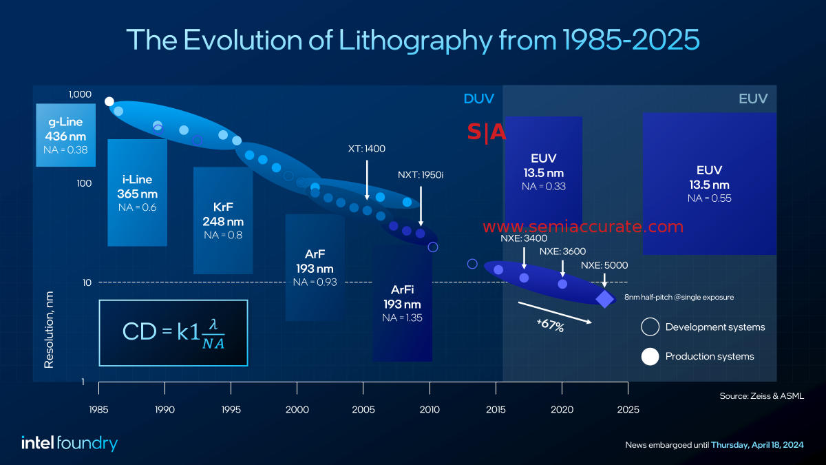
You can see where we are going
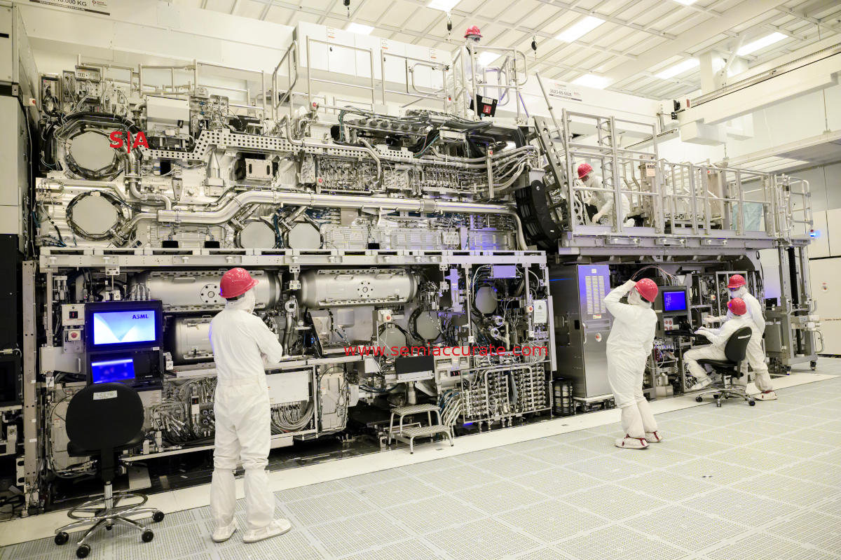
As you can see the NXE: 5000 is a serious tool. What you can’t see is the majority of it that is below the floor, this is one big device. Since cutting boxcar sized holes in fab floors is not usually given the green light, you can see why you basically have to design a fab around the tool, not put it in place once the roof goes on. This is not a simple task.
This is the ‘light’ version, slightly larger than the mobile High NA tools
So the tool is now in place and getting brought up to speed. While Intel hasn’t achieved first light from the tool, they are getting close. It has been assembled and is being calibrated, not an easy or quick task. Luckily ASML did a really smart thing and reused a lot of the modules from the earlier 3600 line in the 5000 so the job is much easier. Instead of having to get up to speed on things like wafer module and reticle, Intel can focus, pun intended, on the new bits.
Once all of this is in place, Intel will have the ability to draw pretty lines that are 67% thinner than the NXE: 3400 could. One slide indicates that you could get ~20nm lines out of the older tools but it is unclear if that is the 3400 or the 3600. The graph shown for the 5000 has the lines at an eyeballed ~15nm or so. More interestingly during the brief it was mentioned that the NXE: 5000 could do pattern shaping with directional light. If Intel ever talks about what they are doing here it could be really illuminating. Yup, another pun there.
If things go to plan, these tools are going to make their debut in the 2025 time frame on the 14a process. Intel has said that a new ‘node’ entails a 15% or more performance increase so you have a ballpark figure to base what 14a is going to be. Intel claims this will bring it process leadership but, well, TSMC isn’t sitting still either. Game on.
The last bit that came out of nowhere was when the presenter said the magic words we have all been waiting for. He said that Intel plans to stack transistors. Really. No details on when or to what degree but it is officially on the roadmap now. Unofficially anyway.
So there you have it, the debut of a customer High NA EUV tool. With it features will get smaller, ASML can draw 10nm lines with a pathfinding version in their labs, so the future direction is coming into focus. The NXE: 5000 should allow Intel to make a cheaper 14a process with higher yields, the theoretical best of both worlds. Stay tuned.S|A
Charlie Demerjian
Latest posts by Charlie Demerjian (see all)
- Qualcomm Is Cheating On Their Snapdragon X Elite/Pro Benchmarks - Apr 24, 2024
- What is Qualcomm’s Purwa/X Pro SoC? - Apr 19, 2024
- Intel Announces their NXE: 5000 High NA EUV Tool - Apr 18, 2024
- AMD outs MI300 plans… sort of - Apr 11, 2024
- Qualcomm is planning a lot of Nuvia/X-Elite announcements - Mar 25, 2024