![]() 3D NAND flash is imminent and Applied Materials is quite excited about the upcoming transition because the technologies involved plays to their strengths. At their analyst day last week the company walked through the process of making 3D flash and went in to how they are solving some of the associated problems.
3D NAND flash is imminent and Applied Materials is quite excited about the upcoming transition because the technologies involved plays to their strengths. At their analyst day last week the company walked through the process of making 3D flash and went in to how they are solving some of the associated problems.
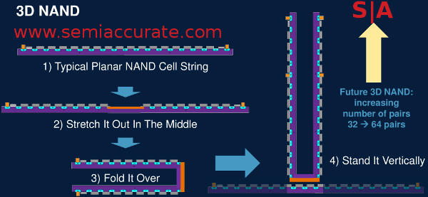
The idea is simple, instead of making a flash chip in a planar fashion as has been done for years, make it vertically and call it 3D. This isn’t 3D as in Intel’s 22nm FinFET/Tri-Gate process, it is really 3D with flash cells stacked on each other 32 deep or more. This rather simple sounding change has more problems with it than you imagine from materials to engineering to physics. Lets take a look at some of them in more detail.
Here is not how they do it
The idea is easy to grasp, take what was a planar structure and turn it 90 degrees to form a vertical stack. In the slide above you can see the process on the flash cell side, this is only a conceptual model though, they don’t do that literally. On a very basic level the flash cells are laid out like they always were, layer by layer with selective deposition and etching. The first major change is that instead of doing one transistor layer then metal layers above it, you lay down 32+ layers that are all mixed transistor and metal, or possibly alternate between transistor, metal, transistor, metal many times. Most companies are not willing to spill the secrets yet but those will be readily apparent as soon as they hit the market.
More technical stairs to climb
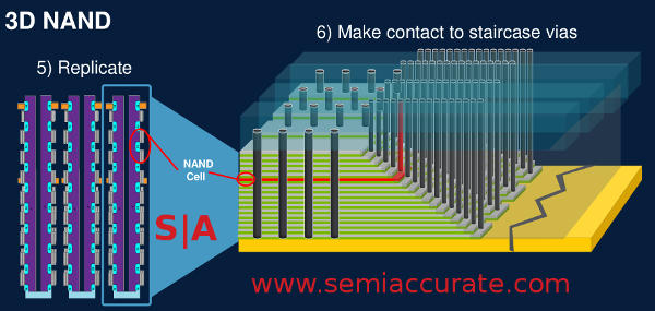
As you can see the first headache is how do you get the power and signals to and from the NAND cells? In a planar structure you just put a contact on top and attach the metal layer on top to it, easy enough. Vias are old hat and so are metal layers. In 3D NAND that space is occupied by another NAND cell so you have to go out the side with your traces. Again this is not a conceptual problem but routing them off the side of the chip is not going to work, if nothing else there is going to be another NAND cell stacked in the way. What do you do?
The solution to this is again conceptually simple enough, you turn the traces 90 degrees and point them up like they would be in a traditional planar NAND device. Easy to describe but how do you do it? Staircase vias. Brilliant. How? Staircase etching. You put down as many layers as you need with horizontal traces then etch them out layer by layer forming a staircase pattern. Then you put in vertical vias down to these exposed horizontal traces and voilà!
Stairs can mean problems for some
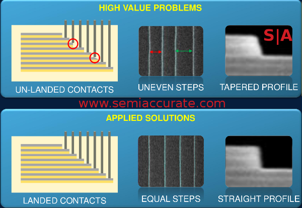
Needless to say this is not exactly an easy thing to do. The concept is simple but etching dozens or more layers without doing things like tapering the edges, having uneven steps, and other cell or chip killing errors is not easy. Doing this on one layer for FinFETs is hard enough, doing it 32-layers deep is a whole other issue. If nothing else the bottom layers are going to be etched in a very deep hole, getting the bottom without nicking the top is not a trivial engineering challenge. Then there is building up the traces, filling in the areas you just etched out, and many more extremely touchy steps associated with the process. If you think about it, if you have a 99% yield on a planar device, what is the yield on 32 layers? .99 ^ 32 is a bit above .72, .98 ^ 32 is a little above .52, and I don’t think anyone gets 98% yields with any regularity.
Why does this engineering problem excite the good folk at Applied Materials? As their name may suggest they apply materials to things usually in the form of layers. More layers means more work for them, that goes without saying. Added precision also is a benefit because minor problems can literally stack up, a-little-bit-off multiplied by 32 becomes much more than a little. Given the tolerances that flash process have in the bleeding edge nodes, a little is likely too much to begin with, 32 littles is right out. That is where one of the less obvious parts of 3D NAND comes in to play, lithographic geometry rules are relaxed when you go 3D.
Yes you heard that right, if you are building Flash at the 19nm node as most of the big players are, going 3D allows you to use ~50nm litho structures/rules. Why? If you think about it litho rules governed the size of structures in the X/Y plane. As long as you were not drawing dots at 19nm you likely only had one of those dimensions constrained to the minimum feature size, think along the lines of an, umm, 19nm wide line that is tens of nm long. Only one dimension is constrained by the litho rules the other is significantly larger.
Litho is expensive, slow, and hard to do right, plus it gets harder the smaller you go. If you take the devices you are building and flip them vertically 90 degrees, you can either do it along the axis that is constrained or the one that is not. With some clever engineering to align all critical widths so they fall on the Z axis what was a painful litho problem almost vanishes. What was a 19nm constraint is now 2-3x that, in the semiconductor world this is about as close to magic as it comes.
This is not all puppies, kittens, and lollipops though, this lithographic gift is accompanied by a dark side. Those critical litho dimensions are no longer a litho problem, they are now a deposition and etch problem. Instead of drawing a line at 19nm you now have to put down a 300mm diameter layer that is 19nm thick, and the error margins for litho are now the error margins for deposition and etch. Any error on one layer will be compounded by the next 32+ layers too. See the problem? What was a relatively easy problem has now become multiple very hard problem. Think happy ASML but frowny AMAT.
So why is Applied Materials happy instead of frowny about being handed this really tough engineering problem? Well as we mentioned before, applying materials and selectively removing them is what they do and they feel they are the best at it. Moving the critical dimension from something that was done by litho to something that is done by depo/etch means a potentially serious revenue stream for them.

Applied Centris Mesa tool
It also may come as no surprise that they do indeed have a solution for these problems, it would have been an odd presentation if they didn’t. In fact the company has two solutions on the etch side, their Centura Avatar and Centris Mesa devices, basically a high aspect ratio etch machine and a multi-device chamber and stage to use them with. Together Applied says they can etch the 80:1 aspect ratio structures needed for 3D NAND fabrication.
Problems come in 80:1 ratios
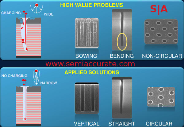
One thing that causes problems with high aspect ratio work is the charge of the chip being etched. If you have any charged particles they will influence the path of the plasma or whatever you etch with causing the problems shown above. Applied says that Avatar very carefully syncs source and bias charges to prevent this leading to much more accurate and vertical structures. Mesa also allows you to put multiple steps in the same device without leaving the vacuüm chambers. With the secret sauce Applied puts in to the Mesa they claim it will reduce uneven steps and tapered edges, the modern high aspect ratio etch equivalent of white shoes after labor day.
Etch is only half the battle however, the other side is deposition. Here too Applied has a full suite of CVD tools and materials both of which are critical to the manufacture of 3D NAND. As we mentioned earlier the critical size rules go from a litho problem to a deposition and etch problem so absolute accuracy is critical. Applied says their tools have a less than 1% variation across a layer and similar precision layer to layer. Lets just say it looks smooth enough to the naked eye but I don’t have a ruler with an edge fine enough to see atomic level variations.
The last part is the materials themselves and of course they have to change radically too. The short version is that when you have to etch deep holes you need to etch either faster or for a longer time. Longer is bad because it decreases throughput but either one is better than not being able to do the job at all. Both also have the problem of needing thicker masks to prevent the good stuff from being etched too, faster or longer mean you need more protection there.
Applied of course has new materials with 2x the etch selectivity of the previous ones for this new task. This means they erode half as fast as their predecessors per unit depth etched. This of course directly translates in to half the mask thickness or twice the depth etched with the same thickness as the old materials. When you are going to 60 or 80:1 aspect ratios, this is not just an academic problem.
In the end going from 2D to 3D NAND is a massively complex undertaking with new tools, materials, and processes involved. The hardest fabrication problem, tiny structures, goes from being a litho problem to a deposition and etch problem, a new world for the fabs. Applied Materials has solutions for each step and luckily for them there are a lot more steps than with 2D NAND. If they have the tech works out the way they say it does, business should be quite brisk for the next few years.S|A
Have you signed up for our newsletter yet?
Did you know that you can access all our past subscription-only articles with a simple Student Membership for 100 USD per year? If you want in-depth analysis and exclusive exclusives, we don’t make the news, we just report it so there is no guarantee when exclusives are added to the Professional level but that’s where you’ll find the deep dive analysis.
Charlie Demerjian
Latest posts by Charlie Demerjian (see all)
- Qualcomm Is Cheating On Their Snapdragon X Elite/Pro Benchmarks - Apr 24, 2024
- What is Qualcomm’s Purwa/X Pro SoC? - Apr 19, 2024
- Intel Announces their NXE: 5000 High NA EUV Tool - Apr 18, 2024
- AMD outs MI300 plans… sort of - Apr 11, 2024
- Qualcomm is planning a lot of Nuvia/X-Elite announcements - Mar 25, 2024