![]() AMD is announcing their newest GPU called Hawaii or R9 290X today, say welcome to the Volcanic Islands (VI) Family. For the regular SemiAccurate readers out there, this announcement more than anything means that you might finally get the joke.
AMD is announcing their newest GPU called Hawaii or R9 290X today, say welcome to the Volcanic Islands (VI) Family. For the regular SemiAccurate readers out there, this announcement more than anything means that you might finally get the joke.
The short story about the VI line is that there is only one VI product, that would be the Hawaii chip that this article focuses on. Hawaii will be available in two versions, the R9 290X and the R9 290 that due to embargoes and other related stupidities we can’t tell you anything about until a later date that we can’t disclose either. Two questions usually pop up in everyone’s mind about a new GPU, price and specs. Price is $549 so expect the Nvidia GTX 780 to take a radical price tumble soon. Specs? See below
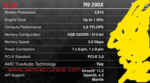
The grand chart of some of the specs, blame AMD for the stupid part
Here are some more numbers for you, 6.2 billion transistors on a TSMC 28nm process all crammed in to 438mm^2 of silicon. Four Shader Engines (SE) each with one Geometry Processor (GP), 11 Compute Units (CU) in each SE, and each CU has 64 shaders for a total of 2816. Each of those shaders is a third or fourth generation GCN unit, more details later, for now take a look at how it compares to the biggest SI chip, HD7970 aka Tahiti.
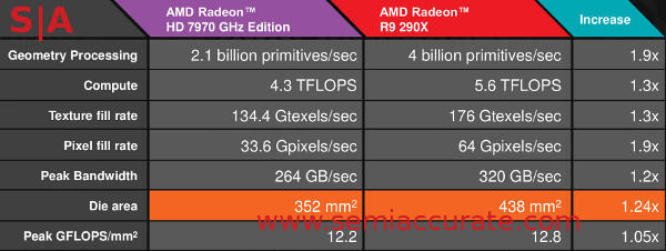
The grand chart of more of the specs
There are more macro improvements like the memory interface which went from 384b to 512b but the speed actually went down from 6GHz to 5GHz in the process. This is a really good thing for buyers, more on it later though. Render Back Ends go from 8 to 16, GPs go from 2 to 4, and L2 caches grow from 384K to 1MB. Hawaii can now put out 64 64b pixels per clock as well and there are more features like TrueAudio lurking under the hood. Hawaii is more about subtle details and efficiencies than big bangs so lets take a look at the details in, umm, detail.
At the lowest level of organization, the shader, Hawaii is almost unchanged from its predecessors. The GCN architecture that first debuted with the NI line years ago is now on its fourth generation with very little differences between now and then. The main thing added to Hawaii is a new instruction called MQSAD or Masked Quad Sum of Absolute Difference with 32b Accumulation and Saturation. If you understand this level of detail I probably don’t need to explain it more, if you don’t it doesn’t matter in your world anyway.
For the inevitable FirePro/professional version of the card the numerical precision has been improved too with native LOG and EXP ops precise to 1ULP (Unit of Least Precision or Unit of Last Place) which AMD claims is 2816 IEEE 2008 compliant. For gamers this means, well squat all, but for CAD aficionados it is important. The DP rate is set at 1/8th SP for product reasons, unless AMD did something radically wrong on this generation the hardware is likely capable of 1/2 rate if uncorked. Yay fusing decisions by non-technical managers.
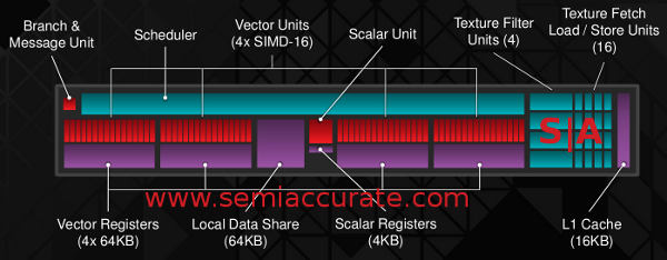
A Hawaii Shader and Compute units looks like every other GCN CU
If you take 64 of these GCN shaders and put a scheduler, branch unit, caches, texture filter, and 16 texture load/store units on them you have Compute Unit (CU) as shown above. If you take 11 of these CUs and put them together they form the basis of a Shader Engine (SE). Doing the math for you, each shader unit would have 11 * 64 or 704 shaders total.
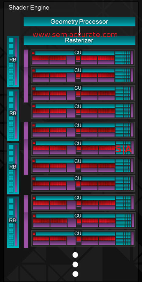
Hawaii’s Shader Engines have 11 CUs
Each SE has a fixed number of hardware units associated with it. In this case each SE has a single Geometry Engine (GE) and a Rasterizer with it, the Rasterizer is pretty tightly coupled with the shaders but the GE is not. Again more in a bit. While there are lots and lots of caches all over the CUs, the 1MB L2 cache is shared by all four SEs. There are also four Render Back-ends (RBE) in each SE but that can be cut down if needed or not needed as the case may be, four is not a necessary number.
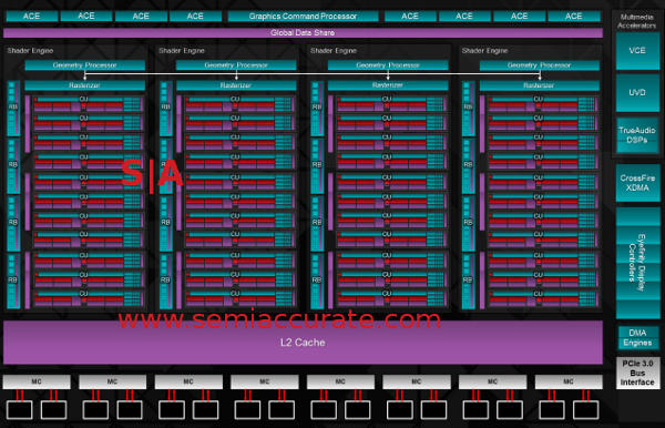
The architectural overview of a Hawaii GPU
If you put four of these SEs on a chip you have Hawaii. Actually there is a lot more to Hawaii than that, starting with 8 Asynchronous Compute Engines, 8 memory controllers (MC) that each have two 32b channels of GDDR5, a Global Data Share (aka cache like thingy), video encode block (VCE), video decode block (UVD), TrueAudio sound, six separate display controllers (Eyefinity), two full DMA engines, and a Crossfire XDMA block. This last one is really important but again hang on for a bit as to why.
You know how the number crunching is done at the lowest levels of the GCN shaders but the larger problem is feeding the beasts. Most of the problems in modern graphics, and to a large extent compute, is not stuffing hardware on to a die but to keeping the hardware you have fed. It is a much bigger and more difficult problem than you think. The first level up is the GPs and the macro organization looks like this.
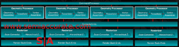
Four Geometry Processors means 4 triangles per clock
As we said earlier there is one GP per SE but the association is not 1:1 as intoned by the diagram. Each GP can feed geometry to any SE which then feeds it to a waiting shader. The GPs are temporally balanced and can send their results to anything that needs it and is open. You might recall that SI GPUs like Tahiti had two GPs and going from one to two is really hard to do, two to more than two is a much easier job. In this case it is probably a simple crossbar.
As a result Hawaii can handle up to four primitives per clock, tessellation can obviously multiply that number quite a bit though too. To keep things from stalling most of the updating work on the VI GPs was in the caching and I/O. The parameter and position caches were enlarged and a load/store unit was put in as well. The idea was that hopefully the results of the tessellation process always stay on die and for the most part Hawaii achieves that. If not the off-chip buffering was also greatly improved at least as far as efficiency is concerned.
In the full architecture diagram the very top line had 8 ACEs and one Graphics Command Processor (GCP). Like the older GCN based GPUs the GCP is there to distribute graphics workloads and the ACEs are there to do the same for compute workloads. Eight to one should tell you about what modern graphics workloads entail, putting triangles up on the screen is the relatively easy part, tweaking them and adding all the effects that a modern GPU is capable of is the complex part.
Things get really interesting when looking at the ACEs, all 8 of them. Their function didn’t change much, once again they are a command processor and parser for compute oriented workloads. On the other hand their form changed a lot, as did their arrangement. AMD didn’t really talk about the CI generation, that would be the one chip called Bonaire, but it all started there and Hawaii is mainly an extension of that.
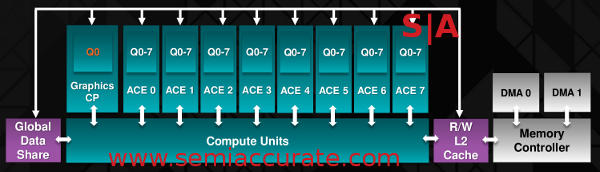
8 ACEs means much more compute throughput
Each ACE is independent and each ACE has up to 8 queues associated with it and can access the L2 and GDS for data. They also work in parallel with the GCP so you can have a total of nine independent instructions handed to the CUs per clock. With 8 queues each ACE is effectively eight threaded as well so there can be a lot of threads in flight before a higher level of software has to get involved.
Task switching on the ACE is temporal, after a set number of clocks or instructions it goes on to the next one. If a queue runs dry or is non-existent it is obviously skipped over so the latency is a little variable, think slightly intelligent round robin. Needless to say the switch latency is extremely low, likely zero in effect due to pipelining. Each queue is just a pointer to the frame buffer or even main memory and do note that in Hawaii the entire memory space is flat.
Each ACE has access to all of the CUs and like the GPs if there is a task ready there is almost assuredly something waiting to work on it. ACEs having access to every CU is a major step towards utilization efficiency, it will be interesting to see how well it does when independent benchmarks come out. It will be far more interesting to see how it does when Kaveri is released too, but that is a bit off topic.
Another associated bit is the aforementioned memory controllers and dual DMA units. The memory controllers are claimed to be far more efficient and use 20% less area than the 384b controller in Tahiti. 20% faster and 20% smaller seems a bit odd for a 33% wider controller but the reason for it is quite simple, powers of two. With a power of two memory width there was no need to put crossbar in front of the memory controllers so that area was saved. Not having to make a few extra switches also means faster and lower latency throughput as well. The dual DMA engines can saturate a PCIe3 16x bus so getting data on and off the card itself shouldn’t be a problem either.
The memory controller architecture is based on those in Bonaire with only minor changes but Hawaii runs them significantly slower than the two generation older Tahiti. Why did we call a 5.0GHz GDDR5 interface a good thing earlier? Easy, Bonaire had a screamingly fast memory controller, it wasn’t hard to find one that would clock to more than 7.0GHz, way more, if you had the right memory. This wasn’t golden sample or hand polished memory just vanilla chips and random memory would often overclock like mad. So think about a cleaned up version of that, twice as wide and clocked very low. Then think about the special edition 290XXX’s or whatever that will surely come out soon. Then grin.
Last up before the pixels go out, that would be 64*64b pixels per clock to the screen, is the Render Back Ends (RBE). Not only is the count doubled but they can also do 256 Z tests/stencil ops per clock now too. Why did AMD beef this part up after leaving it pretty much alone for quite a while? 4K. We told you about AMD’s 4K advances like VESA Display ID v1.3 earlier, and there are some Hawaii specific advances there too like single cable 60Hz support. Unfortunately after the massive stupidities around the partial disclosure and embargoes like being able to talk about the 290X but not the 290, we can’t be bothered to go into detail. If AMD ever decides to not play disclosure games they will probably get us to care about more things like this in actual detail.
The last major component of Hawaii is probably the most important part, the new Crossfire XDMA engine we hinted at earlier. There is of course no Crossfire connector on Hawaii/VI, if you see one it is an older generation chip. This removal of a connector may seem like a loss but the result is much better performance and reliability. Since AMD doesn’t have to bundle a little connector widget in the box either it is also marginally cheaper but that doesn’t matter much on a $549 GPU.
The XDMA engine marks the largest single overhaul of Crossfire since it’s inception. You might recall that the old way had the card that was connected to the monitor pull data from the other cards directly in to the display engine. It was a just in time pull, a fully rendered image was grabbed and stuck in a very small display buffer with really tight timing tolerances.
If there was any hiccup or delays the frame could be missed, something that is more than a theoretical problem. If resolutions were high there could also be overflow problems as well, and again this isn’t theoretical. Crossfire pre-VI has a ton of potential problems and as frame rates rose and display sizes increased, things became even more tenuous. In short the current timing based implementation was running out of gas very quickly.
Enter XDMA, exit connectors, all needed data is now pulled over the PCIe bus via DMA. A requesting card can reach out to the required target and essentially grab, or at least ask nicely, for what it needs. This also allows for an unlimited number of cards in Crossfire but we forgot to ask how many. In any case eight cards should be doable if something else doesn’t bottleneck things first.
What is the XDMA engine? It is really just a display controller connected to the display engine so it can be timing aware but unlike the older way it isn’t timing dependent. This is a subtle but key difference. The card with the monitor connected is now able to prefetch the data it needs long before it needs it. The old Crossfire basically requested when it was needed, not before, and if anything burped things got ugly. The new XDMA version has much more flexible algorithms to both predict and fetch what it needs long before it needs the data. Storage is also larger and more flexible, again based on algorithmic control rather than fixed.
In short as soon as a render surface is enabled on the displaying card the data can be requested from the source. The storage space is also guaranteed to be adequate as well and nothing is just in time delivery so minor bumps in the night don’t turn in to missed frames. This should not only allow more scaling for card count, display counts, and screen sizes, but also higher reliability too. It will be interesting to see if this opens up multi-card, multi-monitor Crossfire solutions, with a bit of clever software hacks, multiple cards each with connected monitors is at least theoretically possible. Hmmm, Pi.
A few more bits of trivia to toss about on Hawaii starting with those four SEs. They split the screen up in to a tiled area where each SE effectively takes a tile set based on a lot of different metrics. Effectively the GPU internally load balances across tiles and SEs but since this is all quite internal and will never be exposed it is only trivia. Given the performance of Hawaii it appears to work quite nicely.
Hawaii also supports DX11.2-BS as in DirectX 11.2 is a BS spec. As with 11.1 that basically combined DirectCompute and DX11 but really added zero on top of it, DX11.2 adds such minor details that it isn’t worth mentioning. What it does do however is give the technically illiterate a reason to upgrade from their ‘outdated’ DX11/11.1 cards. Don’t upgrade for 11.2, upgrade for the rest of the goodies that are in the card, there are quite a few worthy ones.
One thing you may notice we completely skipped was any mention of clock speeds, 947MHz max in this case, and TDPs. There is a really good reason for that and it is called Powertune. Actually the older cards had Powertune too so this should be called Powertune Two too. Or Powertune Three or something, we’re not sure what generation is what anymore. That said the new version is enough of a massive change that it makes clock speeds and TDPs kind of obsolete and deserves an in-depth look that is well beyond the scope of this article. Stay tuned.S|A
Charlie Demerjian
Latest posts by Charlie Demerjian (see all)
- Qualcomm Is Cheating On Their Snapdragon X Elite/Pro Benchmarks - Apr 24, 2024
- What is Qualcomm’s Purwa/X Pro SoC? - Apr 19, 2024
- Intel Announces their NXE: 5000 High NA EUV Tool - Apr 18, 2024
- AMD outs MI300 plans… sort of - Apr 11, 2024
- Qualcomm is planning a lot of Nuvia/X-Elite announcements - Mar 25, 2024