![]() Disco makes devices to process wafers such as saws, grinders, and processing tools but the results are quite exceptional. SemiAccurate has found the processed wafers from their tools fascinating for years and we think you will too.
Disco makes devices to process wafers such as saws, grinders, and processing tools but the results are quite exceptional. SemiAccurate has found the processed wafers from their tools fascinating for years and we think you will too.
If you are familiar with chip fabrication technology you are probably aware that wafers are made with hundreds or even thousands of die on them. Once the patterning and deposition is done, the simplified version of what happens is the wafer is chopped up with high precision saws, placed onto a package, and then tested. The order may change and there are usually multiple testing and packaging steps, but the idea of cutting, packaging, and testing is the important bit.
Traditional methods to do this can be problematic in various cases. What if your silicon needs result in a tiny chip, smaller than the width of the cutting blade, how much area are you wasting? If you have a MEMS device, chances are water or cleaning fluid used to remove post-cutting debris will destroy it. Luckily many MEMS devices will be killed by the vibration from the saw blade itself so water is the least of your problems. OK, that may not be a really good up side.
If you backgrind a wafer to 100µ or so, how do you cut it with a saw? At that point the wafer is floppier than a piece of paper and paper is not easy to cut with a rotating saw blade. Traditionally massively thinned wafers were a novelty, the PC space has height to play with so why bother? Well cell phones for one. And stacked memory. And heat, silicon is a great insulator. And TSVs. And I could go on but as long as you realize that the trend is moving rapidly toward large percentages of wafer output being thinned, you get the point.
Last you get into things like wish lists. You may have noticed that almost all chips are rectangular or more often close to square. If you map those shapes onto a wafer, a product you may have noticed is circular, they don’t match up well. That leaves a lot of unused area at the edges, something that gets painful when wafers cost thousands of dollars each. Imagine if you could do non-square shapes or even stagger really large chips a bit so they use the edges more efficiently, that could add many more die candidates on each wafer.
Unfortunately the high precision saws used to chop said wafers up tend to move in straight lines. When you stick a wafer on a carrier to prevent the bits from flying around the clean room, it tends to force straight line cuts so chop one axis, turn 90 degrees, and chop the other. Then remove the carrier carefully, clean and you are done.
While this works well it forces regular rectangular shapes that are lined up on both axis. Non-rectangular shapes are right out. So are multiple size dice on the same wafer. If you don’t think this last bit is important, you aren’t trying to fill a 450mm 7nm foundry. Or make test chips. Or defray fixed costs like masks. There is a pressing need to put multiple size die on a wafer but at the moment it is not a desperate and critical need. It will be in a few years though.
So what does a company do if it is faced with one or more likely a few of these problems? Disco has solutions for all of these problems to one degree or another. Better yet for those of you not making silicon thinned to less than a human hair, then chopped into non-linear but extremely tiny shapes, the results just look cool. To be honest the shiny bits are what made SemiAccurate notice Disco in the first place, the cool tech news came after we asked about the shiny stuff. The pictures and story comes from Semicon West 2011 but the tech hasn’t fundamentally changed since then and it still looks really cool. You will probably figure out why we are writing this now by the end of the week. :)
The first thing you need to do for any cell phone oriented silicon for example is thin the wafers down. Normal 300mm wafers start out 775µm, 200mm are a bit thinner, and 450mm are going to be thicker someday. Cell phones are now sub-1cm in Z-height so after case, motherboard, screen, and the rest, how many 775µm devices can you stack? How well do you think a phone with 1GB of flash would sell, either that or a 9 inch screen size dictated by the board area needed to place enough memory for a 16GB device.
This is the long way of saying you need to stack memory, flash and other things. If you look at a modern mobile SoC, it is guaranteed to be PoP construction.That stands for Package on Package or in layman’s terms a chip stack with other bits that aren’t necessarily silicon in it. Stacking is mandatory in mobile and is almost mandatory in PCs and other devices if you want any sort of memory density. You may not know it or be able to see it directly, but almost everything now has stacked parts. The tech that goes into the stacking may vary widely but the topology doesn’t.

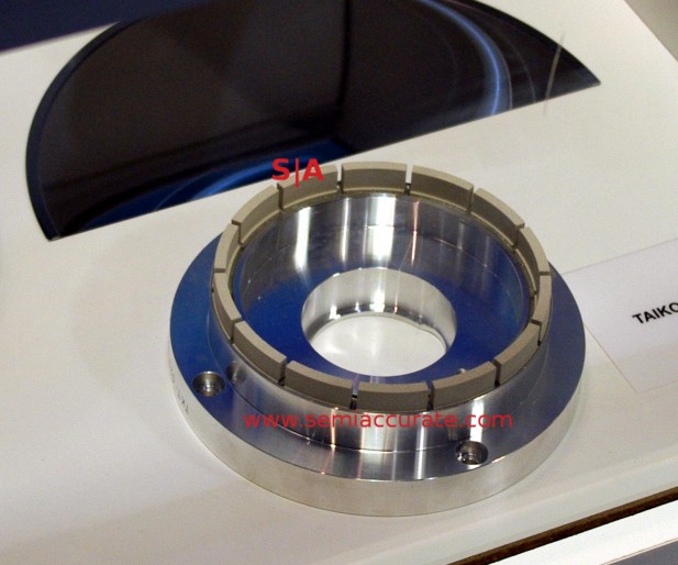
A Disco TAIKO grinder head with a 200mm wafer half
Back to Disco, they have a full line of wafer thinning tools to sell you. These are nothing more than a good old-fashioned set of abrasive heads with tolerances on the scale of microns. That is for both the abrasive itself and the movement of the tool head, something that is not easy to do repeatedly on a 12 inch wafer. If you think of the thermal expansion of silicon and how much heat grinding generates, what are your tolerances again? It is hard work but technically speaking a solved problem for the silicon industry.

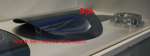
This is why they call it potato chipping
The thing you see above is a standard 300mm 775µm thick wafer that has been background to 50µm with Disco’s TAIKO grinding process. If you are wondering about the shape, when you grind silicon this thin it is no longer rigid, in fact it becomes quite flexible. The term for this is called ‘potato chipping’ and I will leave it up to you to figure out why. Silicon this thin has almost the consistency of mylar or other high-tech plastics, it is really cool to play with. That is why I have a background wafer on my desk, it is shiny and neato.
Back to the serious side, a floppy wafer with delicate far sub-micron transistors on it is really hard to cut to extremely tight tolerances with a circular saw. Actually it is hard to do anything with a wafer like this precisely because it is so damn floppy, not to mention that it likes to curl up rather than lay flat. That is why after being ground, Disco leaves a thin ring of non-ground wafer around the outer edge, it stabilizes the whole thing enough to handle sanely.
From there the wafer is moved out of the grinder and placed on a carrier, usually tape of some kind, for further molestation. The ring can then be removed and the thinned wafer will not be damn near impossible to manipulate. Actually this is vastly simplifying the process but you again get the idea. If you are wondering, a thinned wafer with a ring attached doesn’t fly too well, buy a Frisbee for a fraction of the cost. We don’t have enough objective data to prove this but take our word for it, we did try it a few times for science.
So now you have your thinned wafer that is on a carrier. If you mount it on one type of carrier you can now chop it up with traditional methods and package, test, and whatever else you want to do with it. That is the boring route though. If you have tiny chips and the hundreds of microns of ‘street’ width left by the saw blade may be more area than the chips. This is a serious cost concern.
Luckily Disco has a solution for that too, they call it the Stealth Dicing process and it involves lasers but sadly no sharks. Although you might think that simply chopping up the wafer with lasers is an obvious choice, it isn’t for a bunch of reasons. Those include cost, heat, and time. The electricity needed to cut through a wafer like that is not trivial and adds quite a bit to the processing fees, but it can be done. You have to be a bit careful though because you don’t want to chop through the carrier on the bottom, that would leave lots of tiny, expensive, and hair thin silicon bits floating around.
More problematic is the heat needed to cut such a wafer. Lots of heat will distort edges, can destroy transistors on the edges, and create lots of fine debris commonly called ‘smoke’. Smoke is bad in a clean room environment but it is a solvable engineering problem. Cleaning the debris is too but if you have a MEMS device, it is quite a bit more complex. This all adds up to potentially low yield, wasted area, and high costs.
Disco’s Stealth process starts out with a thinned wafer, 100µm is ideal but you can go up to 300µm economically, after that it is doable but it gets expensive. It starts with an IR laser that is focused beneath the surface of the wafer. The light is pulsed on and off and basically destroys the crystal structure of the wafer under the surface. This does not cut the wafer, it just destroys some of the lattice under the surface.
If you have a thicker wafer you need to make multiple passes at different depths to destroy enough of the structure for the later steps. Each pass adds time, cost, and power so pick your thickness wisely. As an aside, Stealth works with wafers other than silicon, Disco lists sapphire, SiC, GaN, glass, glass + silicon, GaP, LT, and GaAs as workable types too. In short you can probably use it on the type of wafer you are processing.
What you end up with is a perforated line of ‘defects’ running down your wafer so it will fracture easily, something that is good if you want it to, bad if you don’t. The heat and much of the debris is not on the surface of the wafer and if things are planned right, there should be minimal distortion of that surface. This is a good thing. Then you take the tape carrier it is mounted on, hold all four sides and pull. Carefully.
Since laser cutting is not exactly rocket science at the moment, there are some interesting controls you can use. Power, pulse width, head speed, and focus distance are the obvious ones. Better yet you can turn the laser off and turn it back on with very high precision, especially considering the speed of mechanical devices like the laser head itself. This allows you to make cuts that are not straight across the wafer, you can skip areas. Good luck doing that with a circular blade with microns of accuracy.

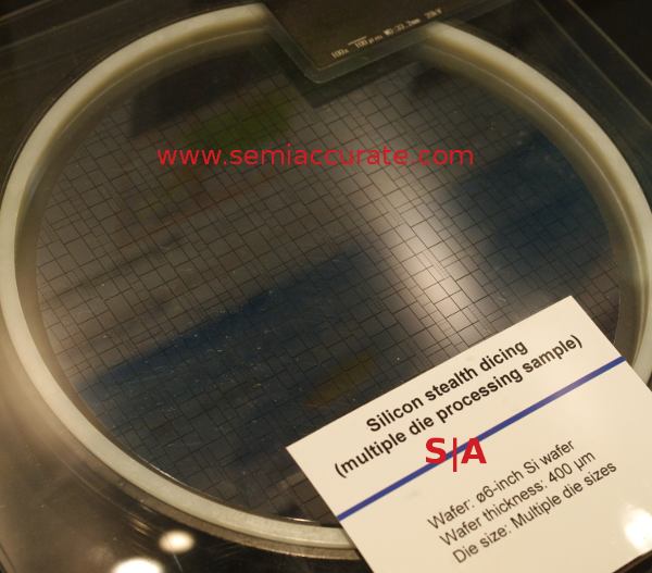
How many different chips can you fit in a reticle?
Turn the wafer 90 degrees and repeat the process to end up with non-regular but still rectangular shapes like the ones above. It may not be as cost-effective as a saw but it solves most of the problems mentioned in the first part of the article. Neat. Better yet when you pull the wafer apart, there is little debris and it is bigger, more contained, and much easier to deal with than that from a saw. About the only thing you can’t do is non-rectangular shapes.

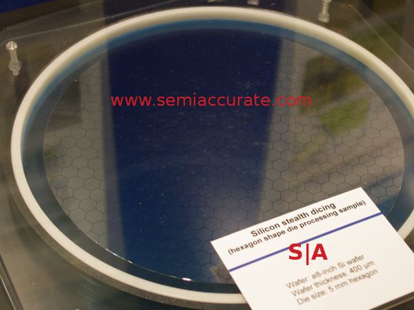
Rectangles are old-school, hex is the new black
Just kidding! You can make non-rectangular shapes with Disco’s Stealth as you can see from the hexagonal dice in the wafer above. Think of the area this could potentially save across a run of thousands of wafers, especially with bigger die. All you need to do is turn the wafer 60 degrees instead of 90 degrees, cut, and turn again. Not rocket science.
Disco was unwilling to say that really complex shapes could be made but that seems to be a fairly simple engineering problem for the motor control guys. The underlying tech is the same if you want to make circles, just turn the wafer and substrate right in realtime and you are done. Hopefully. Maybe.
One real problem is that silicon has a crystal structure that needs to be taken into account. Cutting at right angles is done with the lattice in mind, cutting hexagons or whatnot cuts across the lattice and can lead to serious problems if you aren’t really careful. That said it can be done but non-right angles are actually not as straightforward as we made it sound earlier. If you want to spend the engineering and tool processing time to do it though, you could probably have nicely shaped round SoCs from a round wafer but that would waste scary area.
With those two technologies, TAIKO backgrinding and Stealth Dicing, Disco has solved a lot of the complex and at times fringe wafer processing technologies. Together they open up a huge list of things you couldn’t do before but can now. Some of these like thinned wafers were fringe but are now mainstream, and some are still just fringe use cases. That said you can do it all but the cost of a traditional saw cut is going to be much cheaper for those jobs where the technology fits. As it almost always comes down to in the semiconductor space, it is a matter of cost. If your product can live with those costs, Disco can probably get it done.S|A
Charlie Demerjian
Latest posts by Charlie Demerjian (see all)
- Microsoft Throws Qualcomm Under The Bus Too - May 10, 2024
- Microsoft Absolutely Screws Intel and AMD Over AI PCs - May 8, 2024
- Qualcomm Is Cheating On Their Snapdragon X Elite/Pro Benchmarks - Apr 24, 2024
- What is Qualcomm’s Purwa/X Pro SoC? - Apr 19, 2024
- Intel Announces their NXE: 5000 High NA EUV Tool - Apr 18, 2024