![]() Intel held their Manufacturing Day last week and it seems to be designed to distract investors. SemiAccurate finds the presented numbers odd and uncharacteristic, opinions may differ.
Intel held their Manufacturing Day last week and it seems to be designed to distract investors. SemiAccurate finds the presented numbers odd and uncharacteristic, opinions may differ.
Hyperbolic Scaling:

Hyperscaling is the new black
Intel takes great umbrage to SemiAccurate’s recent characterizations of their messaging so this time we will let the numbers talk for themselves. If you watched the entire manufacturing day you know there was one major theme, a term Intel dubs ‘hyperscaling’. This new technique is meant to keep Intel on the path of Moore’s law even though the gross numerical shrinks have stalled from two to three years and counting.
How Hyperscaling numbers work?
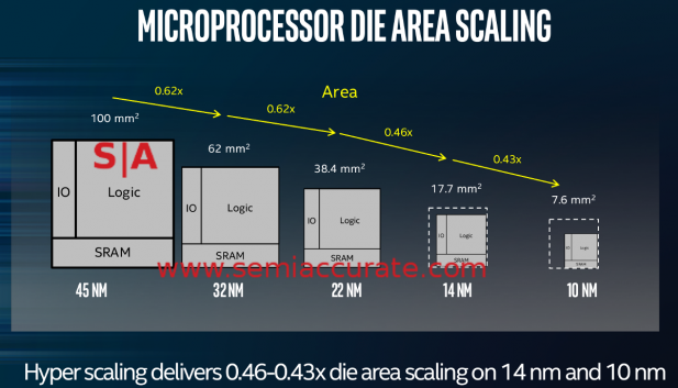
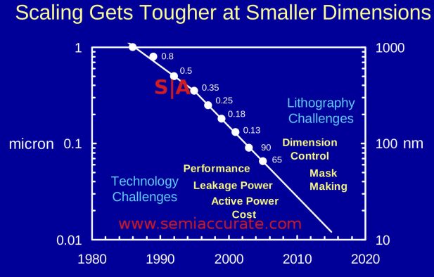
The above slide, Smith’s slide 12 to be exact, characterizes Intel’s claim. This slide, or versions of it, were posted by Stacy Smith, Mark Bohr, Kaizad Mistry, and Ruth Brain. In essence it says that Intel may have slowed down their top line numerical shrinks by 50% but because they do more per shrink, you are still on the same scaling curve. Coupled with a bunch of cost charts, it keeps Intel looking quite rosy.
So in effect what Intel is saying, and why they kept harping on the new term “hyperscaling”, is that they are not slipping in the one area that defines the company. And it’s income, profit, and all the other things Intel is known for. Once again, hyperscaling = no real changes for financiers, everything is normal, nothing to look at, keep moving people, see?
The New Normal:
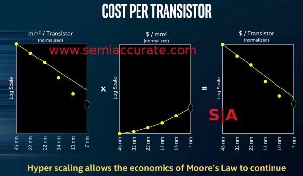
Hyperscaling makes the finances work
Now if you look at the slide above that proves the point. Scaling on 14, 10, and projections for 7nm show a stretching of the timelines but density goes up more than linearly. Cost per mm^2 goes up too, not so great but livable. On the third graph you see the combination of the two points, effectively cost per transistor. That goes down better than linearly, which looks like an excellent for Intel’s future manufacturing, right?
At this point I would like to point you to a single word above all three graphs, the one in parenthesis. That word is normalized, or (normalized). Merriam-Webster defines normalize as, “to make normal (as by a transformation of variables)”. (Note: The same slide from some presenters omits the normalization term but the graphs are the same.) If you aren’t technical this seems to be a pretty simple thing, likely a way of making the data look good for the graph. Nothing to worry about. But is this an industry standard of stating this type of information? Is this a good way to present financially relevant information?
What Intel is doing here is normalizing for yields across processes. Let me restate that for the non-technical, they are saying if yields are the same across all processes, the graphs and numbers above hold true. If you pick a number, lets say 90% yield, the graphs above are true, all is happy, and the finances work. SemiAccurate knows the yields but we won’t disclose them in detail. What we can say is that these graphs are normalized for a reason, yields on 10nm are less that 14nm, 14nm is less than 22nm, and 22nm is less than 32nm. Above that node, most processes are roughly the same for yields. The drop in yields post 32nm are not trivial but we will not go into more detail here.
Intel will not publicly disclose yields, they are a trade secret. Intel will also say that 22nm was their best yielding process ever. When SemiAccurate asked a senior Intel person about what metric he was basing that statement, and the related graphs, on during the 22nm briefing, he replied with a technically correct but largely irrelevant metric. We asked this because at the time SemiAccurate was aware of the underlying numbers and they did not reflect the graphs presented.
Those 22nm numbers were indeed correct but did not tell the whole story. Same for the 14nm briefing. As for 10nm, all we suggest you look for graphs about yields in this presentation and compare their number, frequency, and prominence to those from comparable 14nm, 22nm, and 32nm briefs. You might notice a slight difference in tone and information presented. They also weren’t keen on technical questions from analysts on the topic during manufacturing day.
@CDemerjian they took the mike away from me :-)
— Stacy Rasgon (@Srasgon) March 28, 2017
Yearly Cadence For Now:
Back to hyperscaling once again. Intel is keen to point out that they now are doing updated processes like 14nm+, 14nm++, and so on for 10nm and beyond. These new updates are going to mean continued improvement and keep up the pace of Moore’s law, keep Intel ahead of competitors, and keep costs going on the same or better slope then it was before. No potential financial headaches and the slip for two to three years on overarching process nodes is nothing to worry about. In fact hyperscaling makes it seem like the slip was planned and is intentional, almost a good thing. Is it?
Well if you have been following CPUs for a long time you will know that Intel has been doing two-year process node shrinks for a long time. During the two-year window that a process is leading edge it doesn’t just sit still, there is an update mid-cycle that sometimes coincides with a new architecture. For the past few cycles this has been dubbed tick-tock but it has been going on for quite a while now, just without the name.
Plus is a good thing on process
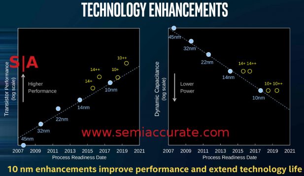
Officially Intel is now doing yearly major upgrades to their processes to bring great advances between node transitions as slide 35 from Mark Bohr’s presentation shows. This ‘enables’ hyperscaling to keep Moore’s law alive despite the slip, so all is well, going according to plan, and not quite the tick-tock-sproing-thud as SemiAccurate dubbed it. The first of these updates to hit the market is Intel’s newly named 14nm+ process which makes Kaby Lake a great thing despite the fact that it was meant to be on a 10nm process and called Cannon Lake a few roadmap revisions ago.
Because of the process updates that are part of Hyperscaling, 14nm+ and the rest, 10nm shrinks were not just unnecessary but also not the best way forward. Intel now has a new way of doing things that blows out the old two-year process shrinks and makes them more money. The slips weren’t so much a problem as a planned change for the better. Again sounds great and yield normalized graphs aplenty show this in simple terms even (only?) a non-technical person could grasp. But there is one point that is important to understand.
What Was Old Is Now New:
When Intel announced the 14nm+ technology, SemiAccurate mocked it for two reasons. First is that they put out fluff rather than any details, facts, or science in a presentation that is meant to be all about hard science. If you think process optimizations and improvements in the far sub-nm area are about fluff and simple graphs, you are in the wrong field. Second is that, quite simply, this is nothing new. Intel has been doing these mid-life process improvements aka PDK updates for years now. Decades even.
Intel is claiming 14nm+, 14nm++ and all the mid-process updates are new and will power them beyond the Moore’s law scaling slips they seem to be settling on as the new normal. They aren’t. Anyone who has followed Intel for a while now will tell you that this is business as usual and nothing has changed, other than the major node shrink slips. Technically that isn’t true though, there is a big change, Intel is branding this decades old business practice now because Samsung, Globalfoundries, and TSMC are beating Intel like a drum in the PR wars.
What do we mean by saying this ‘+’ process is an old normal? Well for quite literally decades now Intel has been putting out an architecture and giving it a mid-life kicker or optimization. You usually see this as a speed bump that gains a bin or two for the consumer. For Intel these optimizations drop the die size a few mm^2 and save costs, improve margins, and maybe allow a price drop as well. It is a good thing for consumers as well as Intel but technically doesn’t fit into the headline shinks of Moore’s law.
One confounding factor in illustrating this practice is tick-tock. With it when there was a second generation of CPU on a process, it had a new architecture and vastly differing transistor count. This made PDK update (IE 14nm -> 14nm+ style) comparisons impossible, Ivy Bridge and Haswell are not directly comparable but the updates did happen. The 22nm process for Ivy Bridge was vastly different from the one used in Haswell, the latter being much more efficient and smaller.
Had Ivy Bridge been laid out with the Haswell PDK it would have shaved a few mm^2 off the die. This may have been done as a cost saving measure to newer Haswell variants but if it was Intel never called it out, and SemiAccurate hasn’t seen any data on it. So what do you have to look for to see if the 14nm+/PDK updates are a new thing like Intel claims or representative of larger underlying issues? You would need to look for those shrinks in the past on a common architecture.
Tick-tock makes this hard. The fact that Intel, to the best of SemiAccurate’s knowledge, has never called out these updates makes it even harder. Topping it off is that few if any analysis companies bother to publicly post teardowns on mid-life kicker products makes it yet harder. Impossible to prove?
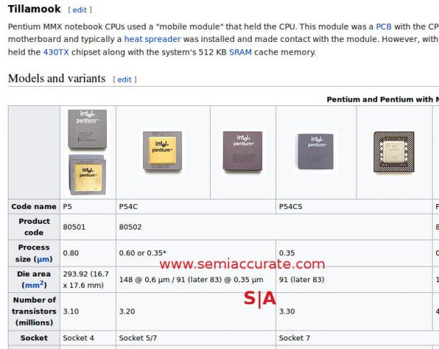
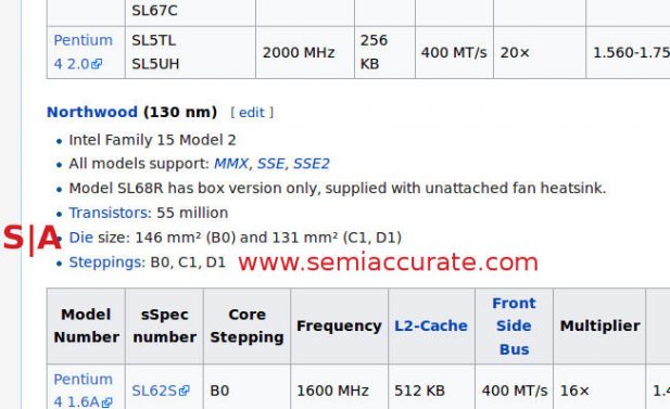
In about 30 minutes of searching, SemiAccurate found two examples. Better yet they are each in different decades to the one this article is written is, the first one being in the mid-1990s the second in the early 2000’s. Note in the above screen grabs of Wikipedia pages, the P54C gets a mid-life shrink from 91mm^2 to 83mm^2 with identical transistor counts and likely a new bin on top. Same for the Northwood Pentium 4, it’s mid-life update shrunk it from 146mm^2 to 131mm^2 again with unchanged transistor counts. In this case you can see the 146mm^2 B0 step had a high bin of 2530MHz while the smaller 131mm^2 and later released C1 upped the clocks to a high bin of 2800MHz.
This is the long way of saying these ‘+’ processes have been with us since at least the mid-1990s. Intel is claiming they are new. It sure looks like they are pretty old. Intel is claiming that because of these new updates the slip for top line shrinks from two to three years are not a big deal. SemiAccurate thinks this is a very big deal. This intones the ‘+’ and ‘++’ variants are stopgaps that have been around forever, Intel is just banging the drum about them now. Please do note that these shrinks are orthogonal to the normalization issues above as well.
To recap a bit on hyperscaling we have two features so far, mid-life process updates and cost curves. Both of these are minor players compared to the third piece, the huge scaling benefits that keep the underlying trends going. Intel is claiming that even though they take 50% longer to do a top line node shrink, the steps they are taking are greater than before so it all works out. Actually these huge steps are so big that Intel is shrinking more than the prior nodes. Take another look at the hyperscaling graph from above.
What’s In A Node?:
Once again, Hyperscaling
Lets go off on another tangent here, how to characterize a node. During manufacturing day, Intel rightly called out their competition for departing from reality on node naming. SemiAccurate has long been critical of this trend and has called out the culprits for years now, this being the most recent example. We have also credited Intel for doing the right thing in this area for the right reasons, a trend that they have only recently departed from.
A possible new way
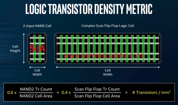
Unfortunately there is no single formula to characterize a shrink. Some use SRAM cell size, minimum drawn line, gate pitch, interconnect pitch, and a host of other specs, but there is no industry standard way to measure a process size. As you can see from the picture above from Mark Bohr’s first manufacturing day talk, Intel is proposing a weighted average of two cells, NAND and a Complex Scan Flip-Flop logic cells.
A specific metric for processes is a good thing but the key takeaway here is that there is no one way of measuring things. Closely related to this is the fact that almost no company calls out what they are measuring with their shrink specifications. So when you look at the Intel hyperscaling graphs, presented below for the third time, there is really no way of knowing what they are measuring or how they are weighting it. One thing SemiAccurate will assume is that the measurement is consistent throughout generations, IE the weighing and base metrics don’t change per node on a given graph.
Hyperscaling for a third time
Scaling Wall Street:
Once again Intel’s new hyperscaling methodology keeps them on a consistent path for Moore’s law and the financial benefits that brings despite the slip in top line shrinks from two to three years. The better than linear shrinks per node mean that even with this slip that is officially not a slip but a good thing, all is great. Stockholders and investors can rest easy.
But notice that scaling trend line change between the 22nm and 14nm modes? On the 22nm and prior nodes, 32nm and 45nm, the scaling was only .62x rather than the Moore’s law expected .5x. On 14nm and 10nm it is .46x and .43x respectively, way better than before hence the need for a new term, hyperscaling. Officially this isn’t just PR and obfuscation, it is real and has tangible benefits as the slides show. According to Intel, it more than makes up for node slips, which explains why versions of this graph were presented by at least four of the speakers at manufacturing day. Hyperscaling, remember the name and the graph.
Luckily for Intel, hyperscaling came along just as the top line node shrink slips happened. It may have taken Intel 3+ years to call it out, but it has been there all along. The cynical who say it is just handwaving, data manipulation, and obfuscation to distract from a technical train gone awry and it’s crippling financial implications are dead wrong. There is a distinct shift in the shrink trend lines between 22nm and 14nm, and that is the savior, hyperscaling. And it has no details about what metrics or weighting were used to determine the shrinks.
Historically Speaking:
Now lets take a look at what Intel claimed in the past before these slips. And before hyperscaling saved them. Specific attention should be paid to their weighting and metrics. In this case we will normalize the slides to graphs presented by Mark Bohr during official Intel presentations. The first two are from his IDF 2014 talk entitled, “14 nm Process Technology Opening New Horizons” specifically slides 7 and 27. Next up we have Mark’s 2012 IDF talk entitled, “Silicon Technology Leadership for the Mobility Era“, slide 4 to be exact. Lastly we have a 2004 press release entitled, “Intel’s 65 nm Logic Technology“, slide 2.
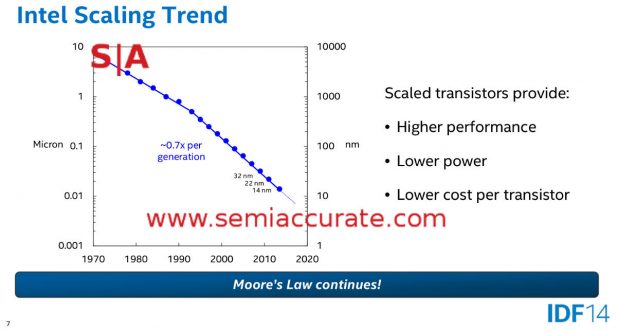
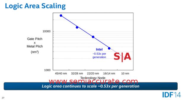
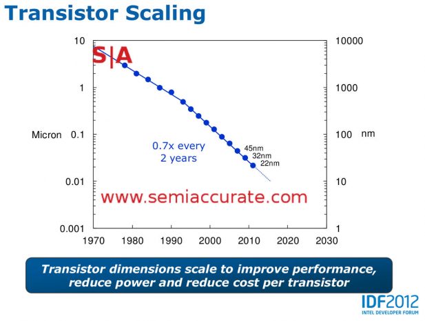
Four slides, one speaker, one company
Notice anything about the slides above? If you look closely, the lines from the 2004-2014 presentations all show the same exact scaling slope of very close to 50% shrinks from .35 micron to 14nm. All have the same knee of the curve at the same node. None show any change between 32nm and 22nm. The 65nm talk obviously doesn’t cover 32, 22, or 14nm it is just there to show historical methodologies that carried over until 2014, at least. The other two do show the 32nm to 22nm transition with measured data, not projections.
What these 2012 and 2014 presentations, again by the same presenter, Mark Bohr, do not show is the shift in scaling that makes hyperscaling ‘real’, effective, and an offset for Moore’s law top line shrink slips. To make matters a little more complicated, all of the other three presentations show a distinct scaling slope of ~.5x (note .7x linear squared is .49x) for decades. One of these includes 22nm, the other includes 22nm and 14nm. In last week’s hyperscaling presentations, all of them across presenters, for some reason characterize this slope as .62x, a non-trivial difference. In fact the 2014 IDF presentation directly calls out this slope, from 45nm to 14nm, as a .53x shrink. Hyperscaling? Also note that the historical graphs on almost every Intel process talk for over a decade are absent in the 2017 Manufacturing Day presentations.
This Leaves a Few Options:
This leaves us with two options for what happened. The first is at manufacturing day Intel obscured actual information about numbers, something SemiAccurate doesn’t think is even remotely the case. We think every number Intel presented is dead on accurate, true, and completely lacking in details and metrics necessary to determine what they mean. But they are dead on true, that bears repeating. As does the part about complete non-transparency for the data presented.
The second option is that Intel changed their metrics without noting it in a clear and comprehensive manner. That audience was investor and analyst heavy and several of the speakers were high-ranking executives of the company. The slopes of the curves unquestionably changed in this presentation, and did so in a way that made Intel look exceedingly good, and fit the new hyperscaling paradigm perfectly. The presentations were meant to dispel the common notion that Intel has been badly slipping in process tech, their competition had caught up and in some cases exceeded their capabilities, but hyperscaling was the answer.
The curves fit the message but do not fit historical norms, conventions, or presented numbers. Nowhere was this called out. In fact the same numbers from the same presenter at IDF three years earlier directly contradicted the message and conclusions of Manufacturing Day, and did so to Intel’s benefit. No changes in methodology, metrics, or processes were called out on either set of slides but one has a 10+ year history of stability, one fits the image Intel wants investors to believe now. That image is that the company is not slipping in process tech.
If you want to argue minutia, you can point out that the 2004-2014 slides measure logic scaling, transistor scaling and other metrics while the Manufacturing day slides measure “Microprocessor Die Area Scaling”. Some might call this a different set of numbers and use it to question the implications of the slides and presentations gathered here. Our reply would be that we agree that the numbers are true, accurate, and correct. The new graphs very well might be different from the old ones, but if that were the case, Intel just deviated from the historical reporting norms in a different way, but the deviation remains.
The Story So Far:
So in summary, Intel presented the term hyperscaling at their manufacturing day last week. It was said to represent a new way of manufacturing that changes a key parameter of Moore’s law, time between shrinks, but shrinks more per gross step. Coupled with a new yearly inter-node process updates characterized by a ‘+’ or ‘++’, the same overall trend lines, and financial benefits, of a 2-year Moore’s law gross shrink cadence are maintained.
SemiAccurate presented data points that these ‘new’ inter-node process updates are not in fact new but are business as usual. They have been going on since at least the mid-1990s with the P54c Pentium processor, continued during the early 2000’s with the Northwood Pentium 4 CPUs, and were obfuscated by the tick-tock methodology in more recent years. There is no question they have been Intel’s standard business practice for decades.
The graphs for scaling that showed off the benefits of hyperscaling are curious data points as well. From 2002-2014, possibly much earlier as well, Intel used a single unchanged methodology to characterize their process shrinks. It showed an ~50% shrink from major node to node for decades, and those nodes were consistently two years for the overwhelming majority of those steps.
When Intel started slipping node transitions from two to thee years and most recently lost the process lead to competitors, they ‘invented’ hyperscaling, an engineering process to make up for it. The numbers presented back up this rosy picture of nothing being wrong. Unfortunately however, historical numbers from the same person presenting the same data for the same company show a very different picture over the past decade and a half, possibly more. Those historical numbers contradict the current message. No change in methodology was called out, and due to the lack of detail in the presentations, you can’t tell what changed. This leaves more qustions than answers.
All of these things back up the three financial graphs Intel presented multiple times at Manufacturing day. Although costs are going up, with hyperscaling the net result is a great benefit for Intel, not the expected losses from node transition slips. This is all quite true if yields are the same or better for newer nodes. Intel normalized the graphs for some reason so you can’t tell what the actual yields are, nor their effect on the financial outlook. If they are far worse on newer nodes as some have intoned, the rosy financial conclusions may not smell quite so sweet. If yields on 10nm are better than 32, all is well. Feel free to draw your own conclusions based on yields for current processes.
So with that we will end by not drawing a conclusion. Last week Intel was quite cross with SemiAccurate about the conclusions we drew about their behavior and ethics on a different topic. Because of this we won’t draw any conclusions about why the data presented at Manufacturing Day differs from historical norms, presents business as usual as new, and has differing slopes for curves surrounding historical data to fit the new public paradigm, hyperscaling. SemiAccurate feels it’s readership is more than technical enough to run the numbers for themselves, research these data points, and come to their own conclusions. One thing we can say about the slope Intel is on is that it sure looks slippery.S|A
Charlie Demerjian
Latest posts by Charlie Demerjian (see all)
- Qualcomm Is Cheating On Their Snapdragon X Elite/Pro Benchmarks - Apr 24, 2024
- What is Qualcomm’s Purwa/X Pro SoC? - Apr 19, 2024
- Intel Announces their NXE: 5000 High NA EUV Tool - Apr 18, 2024
- AMD outs MI300 plans… sort of - Apr 11, 2024
- Qualcomm is planning a lot of Nuvia/X-Elite announcements - Mar 25, 2024