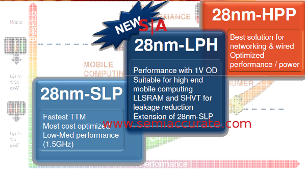
 Global Foundries and Samsung put out a joint release about a new 28nm process, conveniently jointly developed. The process is called 28-LPH, and it is going to be offered by both companies across four fabs.
Blobs on a curve
28-LPH is a middle ground process, half way between 28-SLP and 28-HPP. HPP uses strained silicon, usually done through a SiGe cap, while SLP does not. HPP is faster, more complex, much harder to make, and a lot more expensive per wafer. SLP is the easy one, and those always come first on the roadmap. Roughly speaking, LPH is SLP, IE 28nm HKMG without strain, tweaked for performance, not power savings.
This new process is likely to be used in high end cell phone chips, tablets, and fast A9/A15 type applications where performance is more important than a few mW savings. It also allows for higher voltages, useful for some applications that have higher performance I/O requirements and need things like overdriving. In addition, since LPH is a derivative of the lower cost and ‘easy’ 28nm HKMG variant, it should be out in very short order.
28-LPH will come out of GloFo in Dresden (Fab 1), New York (Fab8) and Samsung in Giheung, Korea (Fab S1) and Austin (Fab S2). Theoretically, the chips from all four places should be physically similar, perform in a similar fashion, and hopefully be able to be dual sourced if needed. Officially, LPH will deliver up to 60% active power reduction or 55% more performance over unnamed 45nm LP variants. As usual, your mileage may vary, but this process seems like a good middle ground between the two older choices.S|A
Charlie Demerjian
Latest posts by Charlie Demerjian (see all)
- Qualcomm Is Cheating On Their Snapdragon X Elite/Pro Benchmarks - Apr 24, 2024
- What is Qualcomm’s Purwa/X Pro SoC? - Apr 19, 2024
- Intel Announces their NXE: 5000 High NA EUV Tool - Apr 18, 2024
- AMD outs MI300 plans… sort of - Apr 11, 2024
- Qualcomm is planning a lot of Nuvia/X-Elite announcements - Mar 25, 2024
