![]() Last week Qualcomm unveiled two new SoCs, the phone oriented Snapdragon 855 and the PC-aimed 8CX. Lets take a look at the first of the new duo and dig into why this one is a big step up in more than the obvious ways.
Last week Qualcomm unveiled two new SoCs, the phone oriented Snapdragon 855 and the PC-aimed 8CX. Lets take a look at the first of the new duo and dig into why this one is a big step up in more than the obvious ways.
If you only look at the top line numbers, both of these new Snapdragons (Snapdragi?) are pretty hefty steps forward in performance and efficiency. While that is a good thing, the most important steps are in the details, both those that bring a big number and those that add capabilities and efficiency. With this new pair of devices you can not only do things you couldn’t do before, but you can do them without draining your battery at eye watering speed.
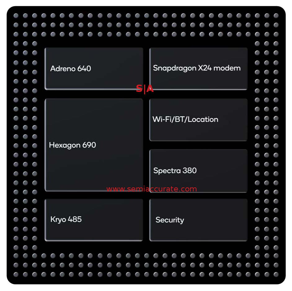
The new vague block diagram
The obvious place to start out with is the CPU which is a lot more than an ARM A76 with a cute logo on top. Qualcomm claims a 40% faster CPU and 20% faster GPU than the Snapdragon 845 which is well withing what the A76 is capable of delivering. What is more interesting is the choices and mods Qualcomm made to the vanilla A76 that make it, well just really interesting.
As you can see above the CPU cores are called Kryo 485 in this generation and they have a not so subtle twist. Like previous generations the cores have subtle mods that improve performance over the standard ARM cores, the ones Qualcomm would talk about is a larger OoO window, better prefetch, and bigger buffers here and there. Between they add up to a not so minor performance boost. Other things like custom integrations with the rest of the CPU weren’t explicitly called out but they are very important on the efficiency side.
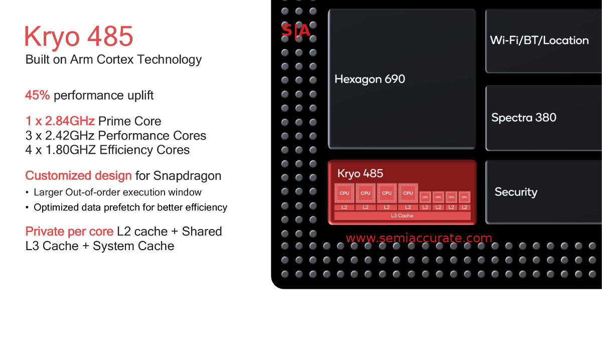
Kyro 485 advances
The biggest bang is what Qualcomm is calling Prime Core or one of the big cores that is bigger than the rest. The Prime Core runs at 2.84GHz while the other three big cores run at a ‘mere’ 2.42 GHz and the little cores can hit 1.8GHz. This means there are three clock domains, one for the Prime core, one for the three big cores, and one for the small cores in case it isn’t too obvious. In a surprise twist there are only two power rails, one for large and one for small cores. Individual cores can be power gated to zero but the voltage remains the same for each CPU in a group. This saves pins, power, and cost.
Clocks are not the only thing different about the Prime Core, it is a completely different physical implementation over the big cores. All of them have a private L2 cache, a shared L3, and a 3MB shared system cache as well, this is pretty standard for an A76-class core. The big cores have a 256K L2 while the Prime Core has a 512K L2, small cores get by with 128K L2. All of this is fed through 4x 16b LPDDR4x/2133 memory, 16GB max supported.
On the connectivity side we have three PCIe3 lanes to plug things into, all of which are spoken for on a fully kitted out Snapdragon 855 system. They are arranged into 1×1 and 1×2 ports and both are meant to connect to external I/O chips. The 2x port is for the X50 5G modem and the 1x port is aimed at an external 802.11ay radio which looks like it could be a minor bottleneck given the 10Gbps the spec is capable of. (Note: We don’t think any first gen 802.11ay silicon will come close to this mark in the real world but if it does you may have to suffer through ‘only’ 8Gbps on that interface.) In any case these are simply PCIe ports so if an OEM wants to use them for something else, they are free to do so. Anyone want a high end phone with a 2x NVMe drive? I do.
Adreno 640 new features
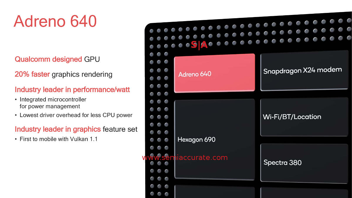
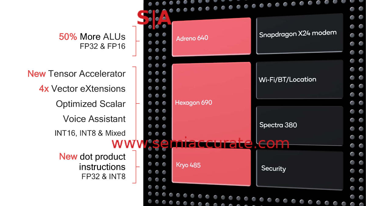
On the GPU side things are a bit more hazy mainly because details were few and far between. The new Adreno 640 GPU is a claimed 20% faster than before for graphics rendering from 50% more ALUs. Because there are no details on the underlying architecture you can assume it is fairly different from the previous few generations, that or the power sweet spot on the 7nm process is at a substantially lower clock. Of the two choices we will go with new architecture, something strongly hinted at by the HDR/10b support added this time around.
Qualcomm was keen to point out the power savings on the Adreno 640 starting with a new microcontroller for power management. Then things moved to software with claims of a much more efficient driver stack that saves a lot of power, something we think is both realistic and long overdue on the PC side of the world. Top it all off with Vulkan 1.1 support which thins out the whole process which directly translates into lower power or at least more efficiency.
Details matter more than ever
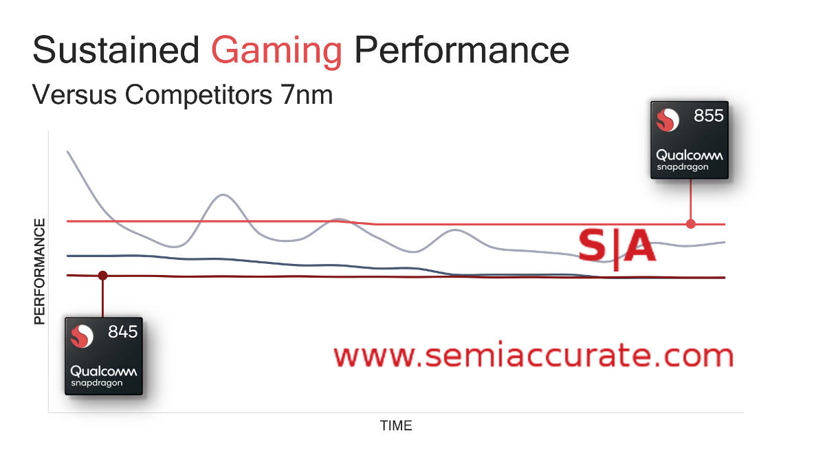
One thing Qualcomm is keen to point out is that their performance is steady over time. This is the long way of saying they don’t use peak performance to game benchmarks, what they claim to get is what they actually get, sustained. With one notable exception in the past few years this claim seems to hold up in the real world. Sustained repeated benchmark running has become a must in the mobile testing world and the graph above shows why nicely. Keep an eye on this in the upcoming 2019 generation of phones, it will show who is sweating the details in a world where details are not a second or third order footnote any more.
More often overlooked when focusing on the screen is the ISP with this version called the Spectra 380. What is new this time is a full computer vision (CV) pipeline that replaces the old way of doing such things on the CPU or DSP. With effects becoming more and more mainstream in modern photography and video, this was only a matter of time.
What the new CV pipeline does is exactly what it sounds like, it bakes the common math and algorithms used in CV into hardware saving power and speeding up the process. The official claims are “extreme speed boost” and “up to 4x power savings”, both sound quite reasonable versus doing the same job on a CPU or even GPU. Areas that are expected to see big gains are multi-object classification, multi-object tracking, object segmentation, CV stabilization, depth sensing on video in realtime, and 6DoF uses. This is a big change that will show up in what you do even if an average user never knows it.
On the speeds and feeds side Spectra 380 is improved everywhere as you would expect from a new chip. It has dual 14b ISPs, supports 2x 20MP or 1x 32MP cameras, supports full Rec. 2020 color gamut, 10b video capture, slo-mo video, HEIF and HEVC support, and a lot more. If you think of the new Spectra as a full 10b wide device capable of HDR everything and supporting modern formats, you won’t be far off.
Moving off of the visual side for a bit we come to AI and there is another big bang here too in the Hexagon 690 DSP. As you might recall from the last generation Snapdragon 845 SoC, there really wasn’t a specific AI block in Qualcomm designs the way there was in some other SoCs. Instead Qualcomm used their pretty amazing Hexagon DSP, GPU, and CPU to do the same work where appropriate but didn’t have a name for it. With the new unit it is called the 4th Gen AI Engine and it has a big twist this time around.
Lots new here
Starting off with the big news we have a new tensor accelerator in the Hexagon 690 so all those whining about names instead of looking at results can now shu… enjoy that Qualcomm has one too. This unit isn’t in the DSP itself but is tightly coupled to it, think a co-processor or accelerator where the DSP dispatches the work and the tensor unit executes it and sends the results back. For specific work that involves lots of tensor calculations, this is going to be a good thing.
More importantly this tensor unit is an addition to the existing AI hardware that was pretty world class before the new kid arrived. That said the ‘old ways’ are vastly improved too as you can see in the picture above. The DSP has 4x the performance as before, Int16, Int8, and mixed instruction formats have been added, and optimizations for common uses like voice assistants are now baked in. Similarly the Adreno 640 has added FP16 and FP32 instructions and the CPU cores have PF32 and Int8 as well.
As we keep saying the benefit of Qualcomm’s AI is in the units as a whole and since there are no sane, non-captive, non-biased AI benchmarks out there, we will just have to go with raw numbers. Qualcomm says that the performance of all the relative units hits a bit over 7 TOPS but what that means is a matter of perspective. On a slightly more grounded note, Qualcomm claims to be 3x faster it was last generation and 2x the performance of the nearest competitor in AI related matters. With the addition of the tensor unit this all seems pretty reasonable.
Now that you have an idea about the AI side of things and the ISP functionality as well, what happens when you combine the two? You get ‘effects’ like depth sensing at 60FPS. In HDR. 4K. Portrait mode in 4K video realtime? Sure. Realtime object segmentation/replacement in 4K HDR video? All of these new units do add up to some useful features but 99+ out of 100 people can’t tell you what AI is doing to make it happen or why.
More importantly if you think about the stunning amount of computation necessary to do all of this, you start to think about energy use. The first Qualcomm SoC to capture 4K/30 was the Snapdragon 800, with the 855 Qualcomm claims it can do 4K/60 HDR with effects and do it in 3x less energy used. Even with the multiple shrinks and their attendant power savings, this is one hell of a leap. If you simply licensed discrete units and slapped them on an SoC you could possibly do the same work but there is no way you could do it on battery power much less do it on battery for a useful period of time. That is what makes the Snapdragon 855 so good, the fact that it can do the bullet points listed in the sales materials in a useful way. I wish there was a benchmark for this.
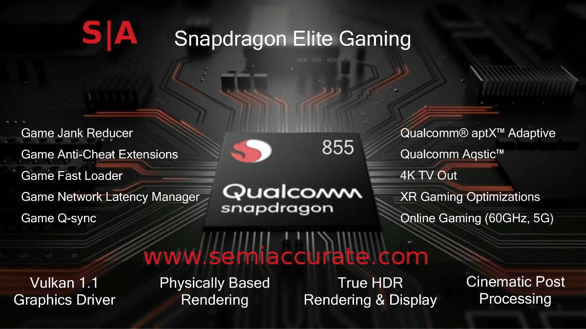
Elite Gaming defined
The next bit is more on the software side of things, remember the Elite Gaming tag from the 855 teaser? This time around Qualcomm added support for Vulkan 1.1 which is good for a claimed 20% power reduction over OpenGL ES. Add in physically based rendering, a lot of ISP based post processing effects, 10b Rec. 2020 color gamut support, and you have the basis for Elite Gaming. Think of it as a pulling together of hardware features, firmware, and software support under a common banner. Other than advertising in certain markets, until there are hard definitions think of it as just a marketing buzz-term.
Last up we have one of the most important updates to the Snapdragon line in years, connectivity. The base 855 has an Cat 20 X24 modem integrated which is good for a rather stunning 2Gbps using 7CA LTE. For the signal geeks out there that is 20 LTE layers and the bandwidth used is…. a lot. All of this is pumped through a separate 14nm RF chip which is one of many in a fully kitted out Snapdragon 855 device.
To officially add 5G you will need a separate X50 modem plus four QTM052 antenna modules if you want to receive mmWave frequencies. Either way the 855 supports the obligatory dual 4G/5G connectivity so we will have none of the pain that the 3G/4G fallback and renegotiation brought to the table. 5G should be fairly seamless and additive when it happens, someone thought this process through.
On top of this Qualcomm is claiming the world’s first mobile Wi-Fi 6 (Aka 802.11ax) solution integrated in the SoC. This one brings 8×8 sounding, target wake up time, and mandatory WPA3 (sort of). If you don’t know what those three things are, you might want to read up on them, they are horribly important to making things not only work but not drain the battery at stunning rates. OK WPA3 isn’t a power use item but it is still stunningly important.
You can also opt for an optional 802.11ay chip for 10Gbps 60Ghz Wi-Fi which breaks the idiotic naming conventions that are just being introduced. If you get an 855 device, try to pick one with the .ay chip, there are some really cool hacks that will probably happen in short order from the location detection/passive radar-like features of the spec. It is worth paying a little more if you are a geek for the chance to play with things like this. That and 10Gbps is a pretty good number for anything, especially at the promised low latencies.

Just a few new items here
As you can see from the slide above, the new Snapdragon 855 SoC has a pretty silly amount of new features, and those are only the big visible ones. There are new units, new features, new pipelines, and it is all built on a new process. Everything is newer, faster, bigger, and better, but it also should consume less energy doing the same jobs as before. On the down side most of this new stuff is impossible to measure in a simple benchmark or report with a number, the devil is in the details and the details are what Qualcomm sweated with the Snapdragon 855. All in all it is looking to be a serious upgrade over the 845.S|A
Charlie Demerjian
Latest posts by Charlie Demerjian (see all)
- Qualcomm Is Cheating On Their Snapdragon X Elite/Pro Benchmarks - Apr 24, 2024
- What is Qualcomm’s Purwa/X Pro SoC? - Apr 19, 2024
- Intel Announces their NXE: 5000 High NA EUV Tool - Apr 18, 2024
- AMD outs MI300 plans… sort of - Apr 11, 2024
- Qualcomm is planning a lot of Nuvia/X-Elite announcements - Mar 25, 2024