![]() Intel ‘launched’ Ice Lake/Sunny Cove last week and in one fell swoop proved just about everything SemiAccurate was saying for the past few years. But they didn’t stop digging there, going on to overshadow everything good about this core while playing up their 10nm woes.
Intel ‘launched’ Ice Lake/Sunny Cove last week and in one fell swoop proved just about everything SemiAccurate was saying for the past few years. But they didn’t stop digging there, going on to overshadow everything good about this core while playing up their 10nm woes.
Told you, again:
Lets start out with a few “told ya so’s” about Ice Lake and 10nm. Remember a bit over two years ago when we said that 10nm was broken and would never be faster than the then current 14nm node? And we showed you where Intel stated this directly in official slides? People didn’t believe it then and still brush the slide below off.
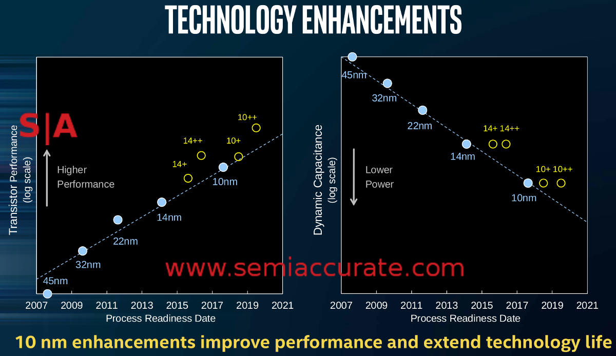
Bohring slide this is not
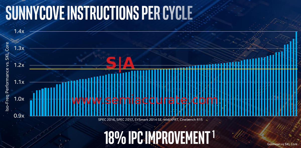
Take a look at this one from the Sunny Cove technical brief. Pay especially close attention to the top left box which shows the maximum core clocks, not the productized version, this was at a briefing about the core itself. Intel for some reason flatly refused to give out any information about the SKUs they launched, almost as if they were embarrassed by them.
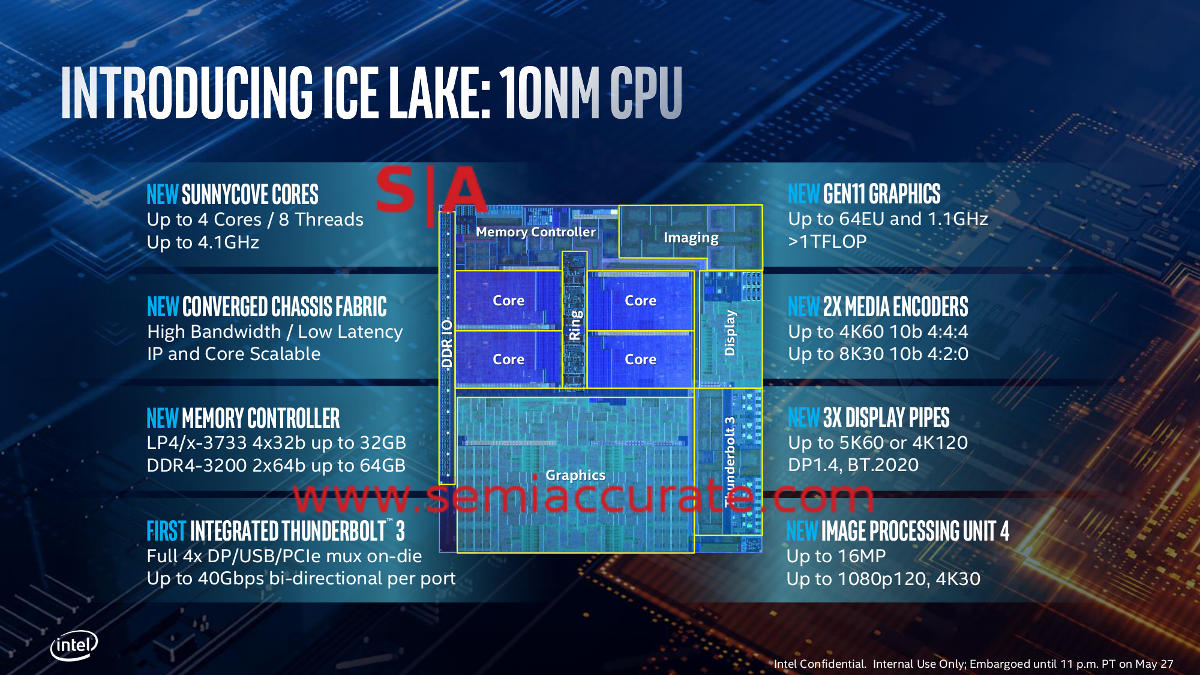
Only 1GHz down
4.1GHz theoretical peak clock is a pretty high number, almost as high as AMD is hitting. Well no, not that high, but high compared to cores from the last decade. Unfortunately for Intel the products don’t hit that theoretical number for some reason, they only hit 3.9GHz. Here are some of the SKUs that Intel refused to hand out.
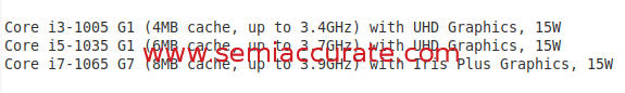 The best of the 10nm lot
Still 3.9 is a pretty big number for mobile parts, right? Yes, unless you look at the current Intel offerings which clock to a mere 4.9GHz. In the same TDP. Whoops. The pic below was leaked in China and SemiAccurate has verified most of the numbers and names. We put a blue dot on the Ice Lake SKU, singular, and a red one on the equivalent, much faster, 14nm part.
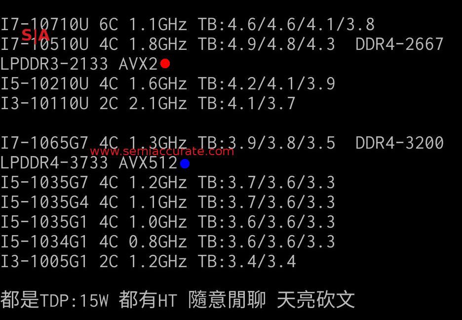
Painful differences
One full GHz slower, can you say death on the store shelves? Now you see why Intel refused to talk product and only wanted to talk tech about the cores? Would you buy a 4.9GHz 14nm 15W TDP part or a 3.9GHz 10nm 15W TDP part for your next laptop? I’ll wait for you to stop laughing to say that things are much closer than they may appear because of the new core. Then they take away any gains with stunts like this in the fine print.
Everything else had specifics
The most positive thing we could get out of anyone at Intel was, “We can reach parity“. 10nm is broken and should never have been released. It is a multi-billion dollar black eye to the company, and why they are publicizing it rather than sweeping it under the rug is beyond us. By stonewalling on the SKUs, Intel ceded any control of the messaging on 10nm and simply can not blunt the impact of this debacle. “Parity” is not enough after five years of delays, no excuses.
Intel can not make Ice Lake/Sunny Cove in any sort of volume and likely won’t until early 2020 best case. Last year they tried an even more embarrassing stunt at launch, and the results were pathetic. This time there is actual volume, all parts of the CPUs sometimes can work, but 10nm still won’t yield at anything close to economic viability. Sandly the cores themselves are pretty good, and if Intel wasn’t so intent on destroying their own image, they could have spun this into something interesting.
The Tech:
What is so interesting about Sunny Cove? Lets start out with the big bang, an 18% IPC increase which is about double that of the last few generation of cores they released. Intel conveniently forgot about Cannon Lake for these slides so it is actually two generational advances so, err, that 18% is about the same as before actually. Still it is a good thing in the absolute sense, much faster and more efficient even if the clock regressions are more than 18%. Net net, good core design hobbled by a broken process.
Not bad but less than clock regressions
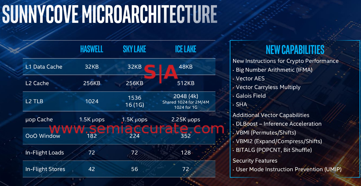
How did Intel get here? By going wide, much wider than before. Allocation is up by one to five, execution ports go up two to 10, more L1 store bandwidth, another AGU for a total of four, plus another store unit for a total of two. In short it gets much wider and that results in a serious IPC gain for Ice Lake/Sunny Cove. It looks like this.
Vague but still lacking
Caches were also improved, the branch predictor was beefed up, and load latency was reduced too. There are a lot more vector instructions including the VNNI quartet from Cascade lake and some other odds and ends. What is really interesting is the killer new AI instruction set called BFloat16 which will make it’s debut in Cooper Lake next year. It is interesting because this next big step in AI speedups is not in Ice Lake client or server, it didn’t make the cut before the design was frozen. Oops. On the plus side Ice has two AVX-512 units, one 512b wide and the other only 256b wide, but this is still a big step forward.
Update June 5 2019 @ 4:05pm: There are two AVX-512 units that are each 256b wide. This means Ice Lake consumer cores can do 2x 256b operations per cycle or 1x 512b which makes a lot more sense than an asymmetric system.
Finally the good stuff
A lot of these increases in performance are easy to explain, a 50% larger L1D and a doubled L2 cache do wonders for hit rates. The TLB gets a healthy increase, the uop cache gets a bump, and in flight loads and stores go way up too. That said if we had to put our finger on the biggest bang here, we would point to the OoO window going from 224 to 352 entries, a more than linear increase over the past several generations. If you add all of these things up you get a much faster, much more efficient core.
If Intel could make Ice Lake yield, and could clock it up, it would have been a really amazing part. Unfortunately if you didn’t get the point earlier, the yields are still non-viable and they don’t clock any closer than 1GHz slower than their 14nm counterparts. On single threaded performance, the hardest metric to improve, Ice is a little better than the Sky Part IV but not enough to notice. Do note the chart below is ISO TDP so the net gain is ~5% on that front.
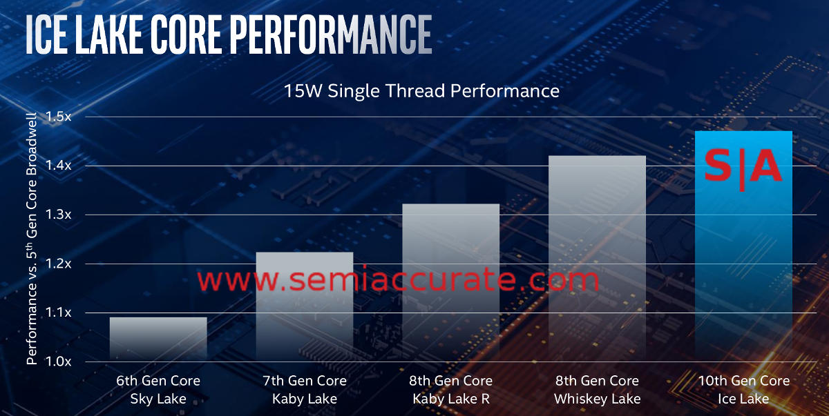
Single threaded performance
Uncore is better too:
Stepping out to the chip itself there are a bunch of additions there too. The new memory controller is the biggest bang with the addition of LPDDR4/4x at speeds up to 3733MHz. The graphics side also has a big increase with the Gen 11 GPU, a claimed 1.12TF from the 64 EUs running at 1.1GHz. This GPU was comprehensively redone from the last Gen 9 parts for a claimed 1.8x increase in frame rates. Not sure why Intel counts 1, 2, 3, 4, 5, 6, 7, 8, 9, 11 though, *COUGH*, but there has to be a reason somewhere.
On the video side there are now two fixed function HEVC encoders that can do up to 4k60 4:4:4 or 8K30 4:2:0. On the output side there are three outs which can do 3x 4K streams, 2x 5K, or one single 8K stream. By the time you buy an 8K panel the silicon should be there to support it, assuming it isn’t artificially crippled on lower end SKUs. Either way the outputs support DP1.4 HBR and HDMI 2.0b so all bases are pretty well covered.
The re-doing of the GPU was not just at the EU level, the cache structure was also heavily revamped. Gen 11 graphics now have 3MB of L3 dedicated cache and shares .5MB with the cores. On top of this the encoders will support 10b widths in hardware which is a pretty big step forward at a commensurately large increase in silicon area. That said assuming everything works as promised, the Gen 11 GPUs should be pretty feature complete. As a side note, Intel appears to have fixed their Linux driver some time in the last year so they are no longer on our don’t recommend list.
There is also an image processing unit and a low power sensor island/DSP on the Ice die. The IPU can process up to 16MP still images or 4K30 video, basically stick with your cell phone on this front. The DSP island is for voice assistants and the like and has been with us for a few generations now but this time around a full quad-core audio DSP has been added. If you are in to having always on mics that may or may not silently send data to people you don’t want to have, this tech will do it much better than the last gen. Yay?
On the I/O front there are some pretty hefty changes too with 6 USB 3.1 and 10 USB 2.0 ports supported. PCIe is still stuck at Gen 3 but there are 16 lanes usable along with 3x SATA6 and an eMMC5.1 port. Our big beef here is that if you want a real GPU on an Ice system you can do it but you can’t have fast PCIe storage too. Which one is more important to you? AMD did a much better job for balanced I/O, on a Ryzen system you don’t have to choose which mandatory feature you want, get with the program Intel.
More interesting is the integration of Thunderbolt, something SemiAccurate first told you about in 2015 albeit for Cannon Lake. There is a large portion of the die which is dedicated to Thunderbolt. This is also the PCIe blocks, TB just adds a little area to the total. Intel claims a substantial power savings with this integration, 300mW peak. Better yet they can now run 8 overclocked PCIe lanes at 20Gbps to the block instead of 17 lanes of 8Gbps for the last gen external parts. If you are in to minutia there are now four root complexes so it is more than granular enough.
Integrating Thunderbolt is a much better and more efficient way to go but no one at Intel is asking the most obvious question, “Why are we bothering to keep this turkey alive in the first place?”. The answer is that it will form the basis for USB4 so others will have to comply, assuming it doesn’t kill USB outright. Time will tell but things don’t appear to be moving in a sane direction on this front.
Smaller, smaller:
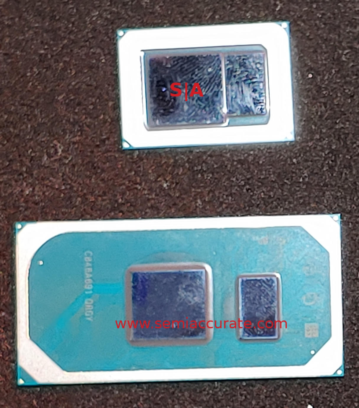
These are really small
On the packaging front things get very interesting. Ice has integrated voltage regulators for the CPU and PCH and thin magnetic inductor arrays. This allows them to fit Ice and the PCH into to multi-chip packages called Type3 (15W) and Type4 (9W). The former is 10x25x1.3mm with 1526 balls on a .65mm pitch while the latter is 26.5×18.5x1mm and has 1377 balls on a .43mm pitch. These are impressive feats of packaging and can even support x64 LPDDR4x memory on PoP configuration.
On the Wi-Fi front things are a bit mixed with the integration of Wi-Fi 6 aka 802.11ax. The functions themselves are not a problem, it is the CNVi 2 connector that gets us annoyed. Why would a link to the discrete AX201 RF chip bother us? Because the link is proprietary and Intel is not licensing it to anyone so it looks like Intel Wi-Fi or more money.
This in and of itself isn’t a problem either but coupled with Project Athena which mandates Wi-Fi6, you might have issues. Luckily there are no slush money games being played with Athena, this year. Wait for it, but don’t wait for Intel to open up that spec. This kind of thing is what ruined the laptop market when Intel forced out competitors with the Ultrabook program. They promise Athena isn’t going to do that this time but all signs point to history repeating itself.
Self-inflicted wounds:
In the end, what do we have with Ice Lake/Sunny Cove? You have a technically solid core that looks better than it is because of the historical whitewashing that is Cannon Lake. It is more efficient than it’s predecessors but unfortunately Intel can’t make it. Volume is borderline non-existent, performance is at best on par with their 14nm predecessors, and clocks, the number that sells to consumers, is down by more than the IPC goes up.
For the next two years 14nm will still be the overwhelming majority of Intel sales. For the next two years, 14nm will still have the performance crown. For the next two years Intel will not be able to make 10nm parts profitably. Intel would not release die sizes or transistor counts this time either so you can be pretty sure 10nm doesn’t live up to their claims. In short Intel shot themselves in the foot again, they designed something they can’t make but won’t stop claiming it is great. It isn’t but it could have been a lot less bad.S|A
Charlie Demerjian
Latest posts by Charlie Demerjian (see all)
- Qualcomm Is Cheating On Their Snapdragon X Elite/Pro Benchmarks - Apr 24, 2024
- What is Qualcomm’s Purwa/X Pro SoC? - Apr 19, 2024
- Intel Announces their NXE: 5000 High NA EUV Tool - Apr 18, 2024
- AMD outs MI300 plans… sort of - Apr 11, 2024
- Qualcomm is planning a lot of Nuvia/X-Elite announcements - Mar 25, 2024