![]() Marvell’s ASIC division laid out some interesting process numbers in a recent briefing. SemiAccurate likes the fact that they were talking about real world cases rather than theoretical percentages.
Marvell’s ASIC division laid out some interesting process numbers in a recent briefing. SemiAccurate likes the fact that they were talking about real world cases rather than theoretical percentages.
We won’t go over Marvell’s ASIC/semi-custom plans again, SemiAccurate covered them earlier, but the summary is they have an interesting IP library and are using it well. During our last chat with Marvell, they talked about being foundry agnostic but were mainly partnered with TSMC on 7nm at the moment. Prior nodes from various foundries were used but the choice of TSMC for the near future was the obvious one.
Today they are actually releasing a set of very interesting numbers for 5nm and better yet it appears to be about as close to the real world as you can ask for without specific product details. Since their ASIC products are designed for customers, Marvell can’t really talk directly about them. As you can see from the two charts below, they can talk about their IP blocks and that gets you most of the way there.
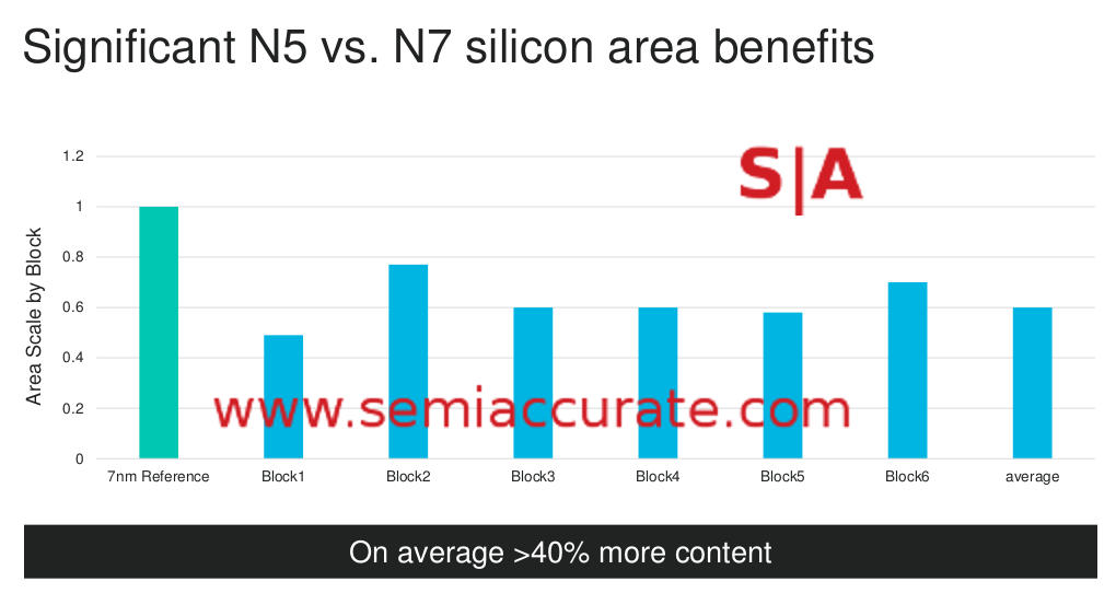
Marvell’s area on TSMC 5nm vs 7nm
First a little explanation. The area chart compares area of a direct port of different functional units of Marvell IP to their normalized 7nm version. In this case a block is not a simple circuit but more of what you would see in a simplified block diagram of a new SoC. A CPU core would be one example, a PHY, DSP, or accelerator are other examples. The scaling factor depends on a number of things, one of the largest is analog vs digital blocks, analog doesn’t shrink well, pure logic does far better. Memory sits in between and depends on a lot of other factors.
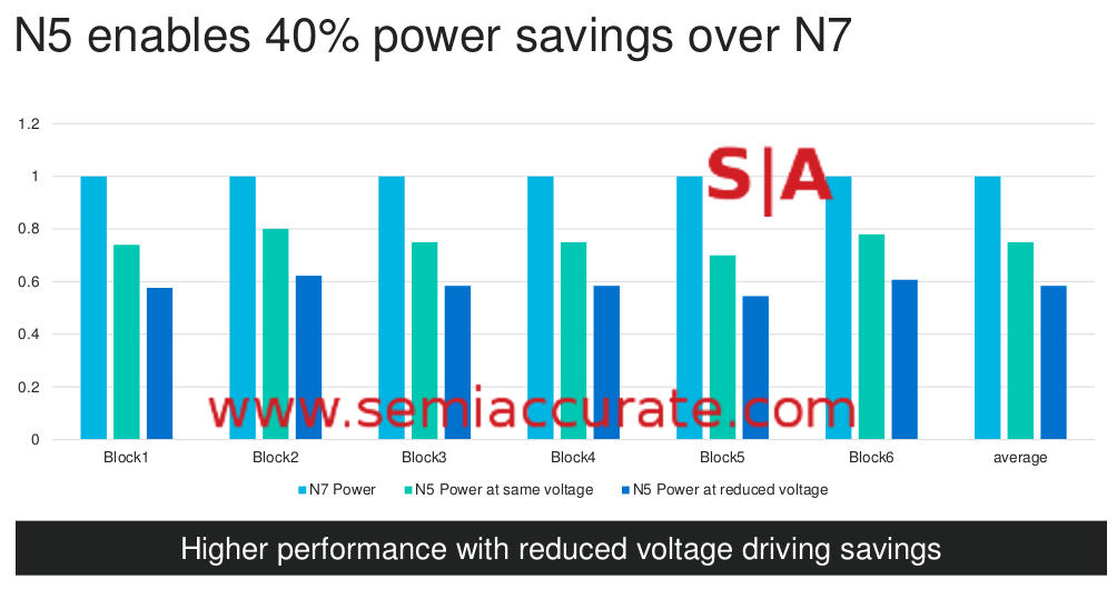
Marvell’s power on TSMC 5nm vs 7nm
The blocks on this slide are the same ones as the prior slide, once again normalized to the same design on 7nm. The middle green column is a simple port to the 5nm and shows a >20% average energy use advantage. If you reduce the voltage to ISO performance you get the dark blue column which almost doubles that average gain. Given that a lot of the ASICs Marvell builds are embedded devices with specific performance targets, this is a realistic scenario.
All of this is interesting but doesn’t really take into account a block built from the ground up to take advantage of the 5nm process. Such a device would probably gain a bit more here and there depending on the exact makeup of the block. That said these numbers are fairly close to what you will see in the real world rather than the nebulous and usually unreachable PR numbers the foundries often lay out. But what does it translate in to for actual devices?
Marvell laid out three scenarios based on the larger vertical markets their ASIC division targets. Below is one based on data center switching SoCs but AI chips and 5G baseband processors were also given similar analysis. The idea is easy enough, you have a performance target and cost target that the customer sets which is represented by the middle line. What is achievable on 7nm and 5nm are on the left and right respectively.
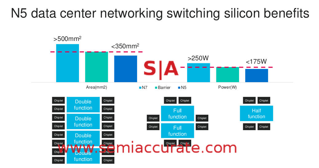
Theoretical data center results
The bits on the bottom are interesting too, basically they are saying that you can stitch those parts together with advanced packaging technologies to make a bigger device. That isn’t anything new but what you probably don’t realize is that Marvell has been doing this for almost a decade. They have been making MCMs for closer to 10 years than 5, chiplets for a long time, and have various memory on package technologies as well. Unfortunately due the the fact that these are not sold as ‘Marvell’ parts, they can’t claim them as their own or even call them out. That said we don’t doubt the claims.
So in the end what do we have? Marvell is talking about TSMC’s 5nm process and doing so with numbers. Better yet they aren’t talking about vague numbers that define the limits of the process technology, they are talking about real world performance and area values for their IP. To SemiAccurate that is a lot more interesting than most technology claims, hope you think so too.S|A
Charlie Demerjian
Latest posts by Charlie Demerjian (see all)
- Qualcomm Is Cheating On Their Snapdragon X Elite/Pro Benchmarks - Apr 24, 2024
- What is Qualcomm’s Purwa/X Pro SoC? - Apr 19, 2024
- Intel Announces their NXE: 5000 High NA EUV Tool - Apr 18, 2024
- AMD outs MI300 plans… sort of - Apr 11, 2024
- Qualcomm is planning a lot of Nuvia/X-Elite announcements - Mar 25, 2024