 Today Intel is launching 3rd Gen Xeon CPUs once again but this time they are based on Ice Lake-SP silicon. SemiAccurate has told you the details before but now it is time for the official word.
History Lessons:
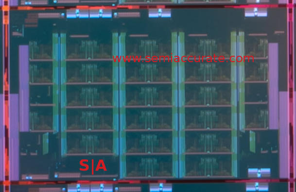
Lets start it out with a little history because this CPU is now two years or so late and a lot has changed since it was first ‘imminent’ in 2019. You might recall that SemiAccurate claimed that Intel’s ‘Ice Lake’ was a mix of 10nm and 14nm devices at that time. What we didn’t tell you was that this was because the larger 42C (at the time) XCC die was canceled due to untenable yields. Cooper variants were slotted in on SKUs the HCC die could not fill. When Cooper was canceled, as SemiAccurate exclusively revealed, Ice Lake-SP XCC was revived.
Notice anything odd?
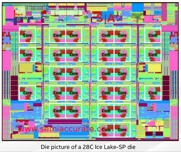
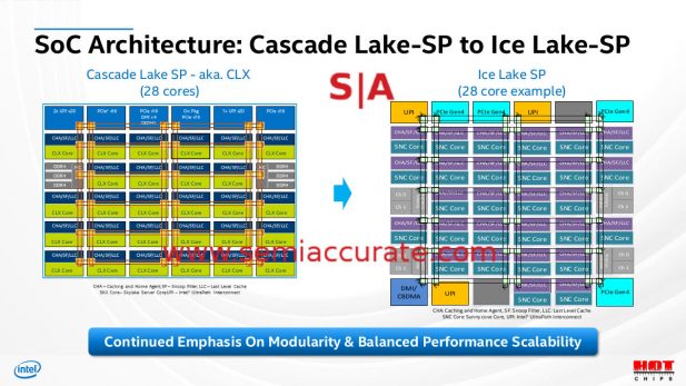
Somewhere along the way this die was re-laid out and two cores went AWOL, you can see the blank spaces all over the die so it appears to have been done with the same level of careful planing as the 5-6 14nm Skylake reactionary updates. If it matters the shipping stepping is D-2 so there were at least three obvious places where this could have happened.
Years before that when Skylake-SP launched, Intel gave preferential early access to a few customers as we exclusively told you. This went over like a lead balloon with those customers not getting the nod, and then blew up in Intel’s face for two main reasons. First is that one big customer sucked up essentially all of the top bin 28C dies leaving little to none for anyone else. A bit later Intel realized that they had to support two microcode/patch streams and on top of that, ran out of space to put the patches. Their response to the customer(s) who needed updates was more or less, “Sucks to be you”. Again, this didn’t go over well either.
That lead to some planning meetings and two things came out of it. First the early access program was killed off for good, something no one really complained about. Second they decided to keep a few cores dark in order to increase initial availability of the top bin. This is why Ice-SP was a 38C part for so long even though there were 42C on die. This was decided on at a time when 10nm yields were still thought to be fixable, it was dropped to 36C when that illusion was shattered by reality.
Out Now, Sort Of:
We won’t rehash the delay, denial, and begrudging admittance cycle that is Ice-SP’s gestation, just be aware that it was a 2019 CPU and is now a mid-2021 CPU. We know it launches today and Intel is officially claiming, “We have shipped over 200,000 Ice Lake CPUs for revenue” and the shipping parts are the D-2 stepping. Since volume production started in mid-January and the throughput is 4-5 months, these parts are likely wafers pulled mid-production and restarted, real production volume is set for May delivery. Don’t take our word for it though, the largest OEM out there thinks so too.
As an aside lets do the math and assume those 200K Ice-SPs shipped in three months or about 66K CPUs/month. If the server market is about 30M CPUs/year, lets call it 32M for the sake of round numbers, that would be 8M/quarter for normal production. 200,000/32,000,000 = .025 or about 2.28 days worth of production. This is not a figure I would be mentioning in public if I was aiming to boost confidence.
Darker Than Planned:
Back to the story at hand, the die went from 42C to dead to 40C over the years, all with good reason. The exposed core count started at 38C lit out of 42 and went to 36/42 for yield reasons. Once again somewhere along the way there were meetings and two press SKUs were put back on the list containing 38C and 40C on the 40C die. Given the yields SemiAccurate has heard for the 38/42 parts, don’t expect volume for either of these versions, they exist for benchmarks and press halos, not sales.
28 cores there for sure
If you doubt this, take a look at the HCC die which has 28C on die according to the Hot Chips 32 talk from Intel. The highest core counts from the HCC dies on the market is 26 on the 5320, XCC dies are used on the 28C 6330 and 6348. That same 40C die is used for volume products down to the 16C 6346, stop an ponder for a second what that says about yields. Don’t forget that a ‘perfect’ 28C is significantly easier to achieve than a ‘perfect’ 40C. Before you point out AMD has an 8C product from 64C candidates, that is for cache, Intel’s cache scales down with lit cores, AMD’s doesn’t.
SKUing Models:
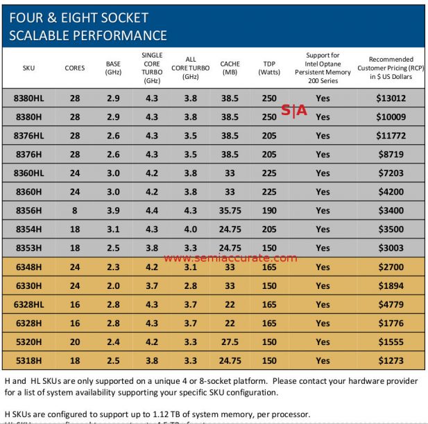
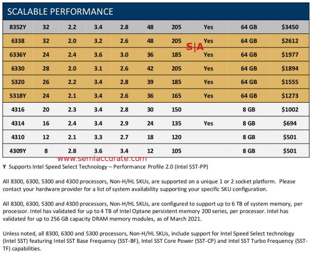
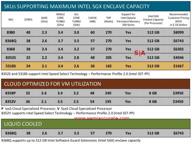
So with that history lesson out of the way, what is Intel launching? A lot of SKUs in 1-8S configurations ranging from $501-13,012. TDPs climb up to 270W even for the liquid cooled 8368Q, it looks like the 300W samples distributed widely a year or so ago have been wisely turned down. In a bit of an ironic twist, AMD’s TDPs actually go 10W higher with the 7003 Milan parts. Before you think something radical has happened, AMD is still ~2x faster per socket but they do consume a bit more power. Back to the SKUs, lets take a look at them.
Update April 6, 2021 @ 3:30PM: The 4/8S CPUs are Cooper Lake/Cedar Isle 14nm parts not Ice Lake based 10nm parts. Sorry about that.
4 and 8 socket SKUs
The first thing to notice is that the 4/8 socket models make a comeback as a separate line after being folded in to the mainstream models with Skylake. Curiously this brought an attendant price hike to all models on Sky/Cascade, something which Intel has been forced to retreat on with Ice Lake-SP. These models bear an H suffix but have crippled memory caps of 1.12TB. If you want that fuse not blown you need to step up to an HL model for an extra $3003 or so per CPU.
On the up side those 4S systems are fully connected since Ice has 3 UPI links per CPU, 8S will obviously not be fully connected but this is no different from past lines. Performance here will be interesting because UPI bandwidth is the glass jaw of Intel’s architecture, it is grossly inadequate for modern workloads and the third link added since Cascade, it was quasi-supported there, was absolutely necessary. If you go to a 4S setup, you drop your inter-socket per-link bandwidth to 1/3 of what it was. Lets see if this shows up in canned benchmarks but the big players are not happy with this. AMD took a much smarter route here.
Optane/Xpoint is supported on 4S models for the first time but once again you have to pay a huge memory tax to get there. All but a few low end 2S SKUs support Xpoint which appears to be more than one SKU per Optane customer. That is a joke, in reality there are probably ten or more unsubsidized Optane customers. Intel talked at length about the wonders of this memory technology, 2nd gen Optane is now available with a new controller. But not new memory. Capacities stay the same, interface speeds go up, prices are still not given out, and still no one cares. SemiAccurate seen some data to suggest that Xpoint is dead at the end of the year but that still may yet change.
Two socket mainstream Ice Lake-SP SKUs
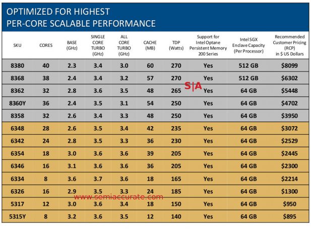
2S SKUs are divided into what Intel calls Scalable Performance and Optimized For Highest Per-Core Performance, slight name changes from the list we published last week. The biggest thing to notice is that Intel is now extorting customers over SGX enclave size, if you want more, you have to pay just like the much loved memory tax. Luckily for customers, no one actually wants SGX at all so no one will actually have to pay. The psychological damage still remains, Intel is making customers realize they are getting inferior products once again even if it is technically irrelevant to them. The own goals just don’t stop with Ice Lake-SP.
Not exactly riff-raff
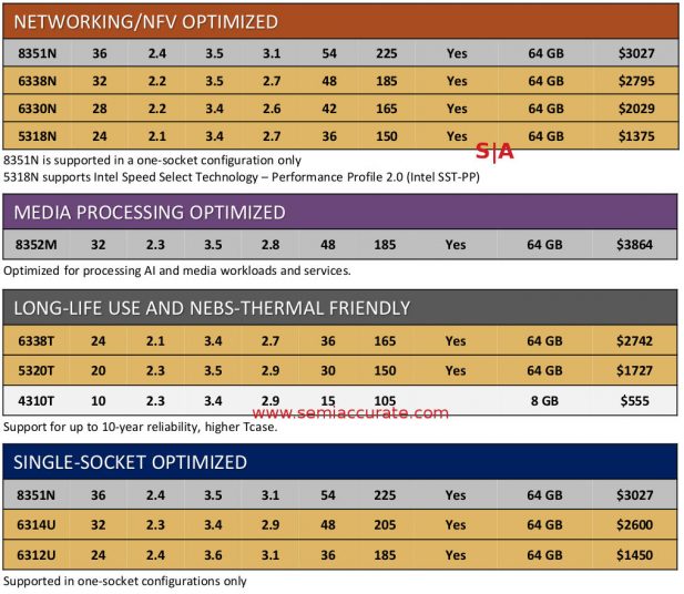
There are some market specific SKUs this time around too but nothing out of the ordinary. Cloud Optimized, Networking/NFV, Media Processing, and Long Life Packaging are essentially carry over lines. The liquid cooled 8368Q is interesting but nothing special, Intel has been pushing for liquid cooling since the Cascade-AP/9200 in order to pave the way for higher TDPs. Expect this to become much more prevalent in the future, TDPs aren’t going down at any vendor. Lastly there are the single socket models, four in fact, running from 24-36C.
Features are hit an miss across the entire line as you can see from the plethora of footnotes. Some SKUs in a line support some features, others have things like SGX enclave sizes arbitrarily fused off, and so on. If you compare this list to AMD’s Milan, the difference is rather profound. AMD is faster, cheaper, and has all features enabled on all SKUs, plus they don’t play games that quite frankly piss off customers in the extreme. It isn’t a contest.
Features Aplenty:
Prepare for eye strain
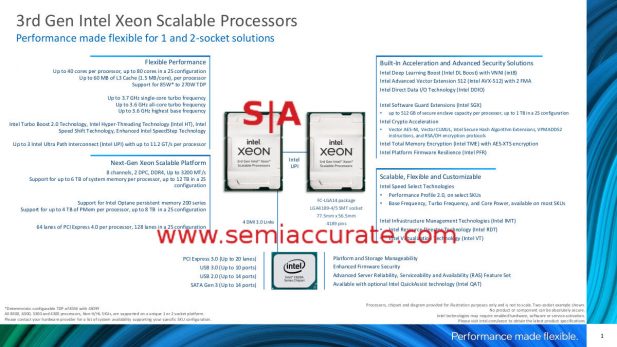
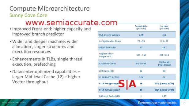
On that happy note lets look at what Ice Lake-SP brings to the table starting with the cores. The new cores are relatives to the consumer Ice cores but have their AVX-512 units bumped up. Server cores now support 2x 512b AVX operations per cycle while the client versions only do 1x 512b operation per cycle. Three UPI links are now officially supported between sockets and there are 64 PCIe4 lanes per CPU so a 2S system can match AMD’s lane count.
Not much new here but still solid
The cores themselves are pretty well known so we won’t go in to those details. Everything is bigger, wider, and faster than before, and the results show a predictable increase in performance. The overall 17% IPC increase claimed by the consumer core seems quite reasonable and bumping up the number of DDR channels from six to eight help to keep things fed. Additionally the memory clocks increase from 2933 to 3200 even at 2DPC but several lines don’t support that speed for marketing reasons.
Overall there is nothing in Ice Lake-SP that stands out as a killer feature. Everything is a little better but the years of delay mean that the overall result is years behind the times. The performance per core uplift is counterbalanced by a clock deficit and a vast increase in energy use. Combined they result in a more or less tie with the older Cascade Lake-SP CPUs on performance per watt, some increase a little, some regress. If you are going to buy Ice, you are going to buy on features like PCIe4, not TCO.
As SemiAccurate showed you last week, there is one SKU with a comparable core count and TDP to Cascade lake, the 6346 vs 6246R, both at 16 cores and 205W. The 6346 runs at 3.1GHz, a 300MHz deficit to the 3.4GHz Cascade 6236R, and Intel claims a 4% performance increase on SpecIntRate2017. Similar comparisons to between the 24C 6336Y and the 6240R, both 24C at 2.4GHz, show a 13% performance increase but the Ice Lake-SP model uses 185W to the 165W of Cascade. Ice isn’t really a step forward unless you look at corner cases.
Corner Cases:
Speaking of corner cases, this is where the story gets a bit ugly. Intel server briefings for the last decade and change have been the gold standard of tech briefings. They had detailed benchmarks, in-depth data, and very precise diagrams. This time none of that exists, the pandemic is being officially blamed but competitive positioning is the real reason. That said if Intel can come up with a good pandemic related reason why the benchmarks the press is usually give were only given to OEMs, we will happily eat these words.
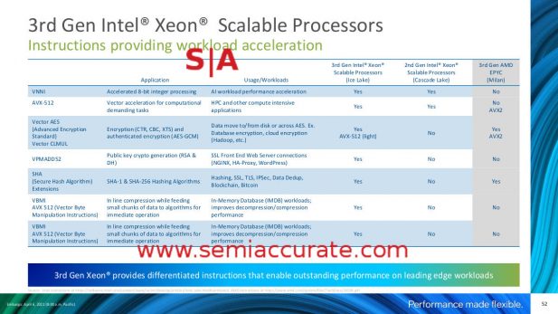
The problem this time around is that those normally neutral, fair, and detailed benchmarks were replaced with an hour of laughably skewed cherry picked marketing numbers. If the real data had been there too, all good, but it wasn’t. It was replaced by version 2 of Intel’s regrettable attack deck, and this time was truly beneath them. While all the data presented was true, it was so misleading it was borderline humorous. Think a 1950’s commercial with the stereotypical housewife of the day professing her love for laundry soap with blue crystals, then attacking her rival for having inferior green crystals. If you are thinking it can’t be that bad, take a look at this slide.
Come on, you can do better than this pablum
Ah yes, Ice Lake-SP has VNNI and AVX-512, AMD’s Milan doesn’t, that covers 6 of the 7 rows. The last is a SHA instruction that both have. Blue crystals are better than green. Nowhere does it mention that no one, other than a few halo customers who Intel likely enabled with armies of engineers, will recompile their code to use these instructions. They also don’t mention AMD pummels Ice in real world testing that these instructions are supposed to support. See Anandtech and Serve The Home for details on those numbers.
Cliplets Again:
Partial truths spun hard
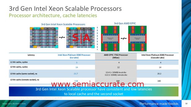
Then there is this one, the old saw about memory latency which we will add is absolutely true. Intel has a monolithic design that allows them to avoid (relatively) slow hops between chiplets. What Intel somehow forgets to mention is that almost no one uses this type of configuration in latency sensitive workloads because it is the worst way to do things, instead users partition. You know, VMs, that newfangled tech that seems to be everywhere now. AMD deployments almost always put a VM or more per CCD so this is a moot slide in the real world.
Similarly non-VM workloads that are latency sensitive will sub-partition their work and pin chunks or threads on a CCD to avoid this issue, you even do it on monolithic dies for the same reason. It isn’t complex, works well, and has been routine practice for years. Intel knows this but conveniently didn’t mention it because blue crystals are better. One then has to question what happens when a workload needs 41 cores, AMD suddenly has significantly lower latency. When you get to 81 cores, Intel has to go to 4S and cuts UPI bandwidth to 1/3rd of what it was, think that will help latency? That brings us to the point we mentioned earlier, UPI bandwidth on Ice is woefully inadequate. Intel’s tests, especially the latency tests are all on lightly loaded or unloaded systems. If you do a real world test, Intel’s numbers like the ones above will likely fall over hard.
No One Does This:
This doesn’t say what you think it does
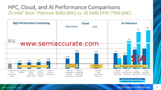
Intel goes to great length to show that when software is rewritten or recompiled with their new instruction sets, it beats AMD’s Milan silly. In this case, Ice-SP does indeed beat Milan silly but as we said earlier, no one in the real world does this, it is too expensive and ties things to one CPU architecture that is significantly slower and consumes more power at everything else. Reworking software like this has no ROI in all but a few corner cases. We feel compelled to point out that this is the same argument Intel spinners were using against ARM a few years ago. Also for some reason, Intel expects customers to optimize for their CPUs but not for the competition, something that strikes SemiAccurate as a tad unrealistic.
Back to the real world
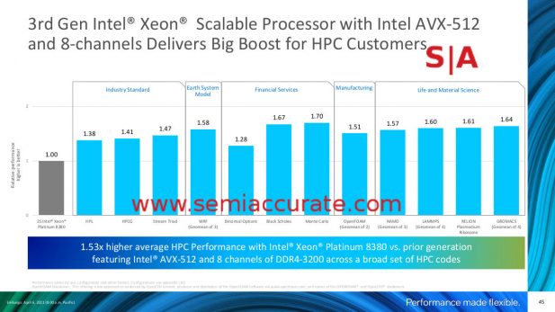
When you look at slightly more realistic comparisons like the ones where Cascade Lake is pitted against Ice Lake, the numbers cluster around 50% performance increases. Since Cascade maxes at 28C and Ice goes to 40C, that accounts for over 40% of the increase, the rest is easily within the core IPC uplift so these numbers seem quite fair. Blue crystals vs more blue crystals seems to be a recipe for honest messaging in Oregon. For some reason Intel completely forgot to test against the 56C Cascade-AP parts, any guesses why?
We could go on about this, there are several more slides that are equally borderline honest. The take home message is that when you compare AMD’s last generation Rome to Intel’s Cascade Lake, AMD was about 2x faster in most real world tests but lost in some single core tests. With the release of Milan, AMD took the single core crown back and kept the core lead. Ice Lake increased the core IPC but regressed on clock and power so AMD still held the single core lead but by slightly smaller margins in most cases. Increasing the core count to 40 narrowed the per socket difference but not by much, anyone who buys on that also buys on performance per watt where Ice essentially regressed. So with no real gains, remove offending data and spin, those bastards with their darn green crystals are, hey, look over there…
Cleaning The Block:
Things like this are no longer provided
Some of the more problematic removals included some of the basics like block diagrams. These have been included in every briefing SemiAccurate can remember for the last 15 years or so but not this time. Why? Dark cores. Intel did put the diagrams in the Hot Chips 32 presentation because they had to, they didn’t have to at the Ice press brief. Die shots and transistor counts are no longer disclosed, nor is die size. Basically anything technical that was table stakes at the prior 10+ briefs was not provided, instead we got blue crystals.
There are a lot more bits that Intel covered in their briefing, most of which were so cursory we couldn’t add anything useful. The rest like Optane 2.0 have been previously disclosed so not much there. The one glaring thing that we didn’t talk about in this piece was security or in this case the lack of. Due to a bike accident delaying writing, this topic will be covered in a near future article, stay tuned, it is a good story.
Overall the message from Intel about Ice Lake-SP is pretty clear, it doesn’t move the needle. On performance per watt it is roughly a wash, outright performance roughly tracks the core count increase, and energy consumed goes way up. Coupled with the platform change, the attendant validation and certification costs make those tepid gains almost a moot point. Layer on Intel’s insistence that Sapphire Rapids will ship this year, it won’t for anything more than PR purposes, and carries a different platform that will be long lived, Ice Lake-SP is a non-starter. PCIe4 on Ice will be replaced by PCIe5 in Sapphire for example, so why jump for six months? Like we said, Intel should not have launched Ice Lake-SP.S|A
Charlie Demerjian
Latest posts by Charlie Demerjian (see all)
- Qualcomm Is Cheating On Their Snapdragon X Elite/Pro Benchmarks - Apr 24, 2024
- What is Qualcomm’s Purwa/X Pro SoC? - Apr 19, 2024
- Intel Announces their NXE: 5000 High NA EUV Tool - Apr 18, 2024
- AMD outs MI300 plans… sort of - Apr 11, 2024
- Qualcomm is planning a lot of Nuvia/X-Elite announcements - Mar 25, 2024
