![]() At AMD’s Datacenter and AI day a few weeks ago, the company stealth announced an HBM Genoa CPU, sort of. In the pantheon of backhanded launches, SemiAccurate thinks this one is up there with the best.
At AMD’s Datacenter and AI day a few weeks ago, the company stealth announced an HBM Genoa CPU, sort of. In the pantheon of backhanded launches, SemiAccurate thinks this one is up there with the best.
Snatching mediocrity from the jaws of victory once again, the product that is a glaring hole in the AMD lineup versus Intel’s Sapphire Rapids HBM/Xeon Max wasn’t touted or even officially admitted to. That said if you look at the technical slides, the product is pretty obvious, as is a lot of the underlying architecture of one of AMD’s most mysterious upcoming devices. Lets take a look.
The impetus for this story came when a fellow analyst in the room asked why AMD’s Instinct MI300A, the CPU+GPU variant, was limited to 4S systems while the new MI300X can go to 8S. Lets set aside the issue that Intel’s Falcon Shores CPU+GPU was demoted to a mere GPU a few months ago, and AMD’s GPU only MI300X was a late addition, but the market has seemingly spoken. That said AMD is still pushing ahead with the MI300A so… so time will tell. Lets get back to the tech though.
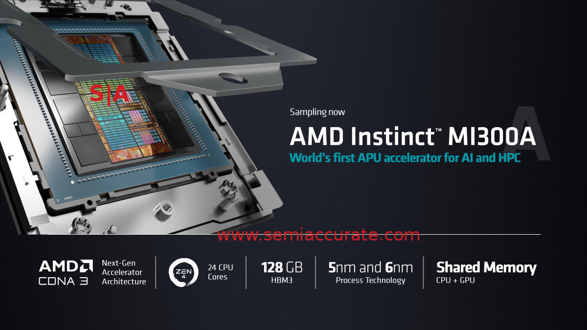
The specs on the MI300A are 24 Genoa Cores on 3 tiles, 6 GPU tiles, plus 4 more for the base interposer/IODs. That said AMD’s technical information on the GPUs were, well frankly pathetic so we may have a lot of the details somewhat off but the grand plan is correct. Think things like the pictures of the GPU having the base IODs wider than the CPU/GPU dies on top. Was that an illustration or the way things are? SemiAccurate was told both yes and no from people who should know. At the time of writing, we still don’t know what it is and have no wish to spend time and effort to clear up the mess that is AMD’s ‘tech’ briefs. That said it won’t affect the premise of the article.
The overarching specs for MI300A, note the tiles
For gross specs, the MI300A has the aforementioned 24 Genoa cores, the same 5nm tiles as the CPU itself, no specs for the GPU because AMD’s tech briefings, and 128GB of HBM3. Those four IODs are made on a TSMC 6nm process, a shrink from the 7nm parts of Genoa. That said they have HBM controllers and the main IODs don’t so calling it a shrink just refers to the process, not the logic itself. Overall there are 146B transistors.
The MI300X replaces the three Genoa CPU tiles with two GPU tiles but ups the transistor count to 153B. It also ups the memory to 192GB of HBM3, the gain coming from higher capacity stacks rather than more stacks, 16GB vs 24GB each. The MI300A is ‘shipping’ now but the MI300X comes in Q3 which is also now due to how late this article is. In any case don’t expect to find either part on the shelf, they are aimed at OEMs and system builders exclusively. Take a look at the MI300AX module and the 8x MI300X Instinct Platform to get a better understanding of why.
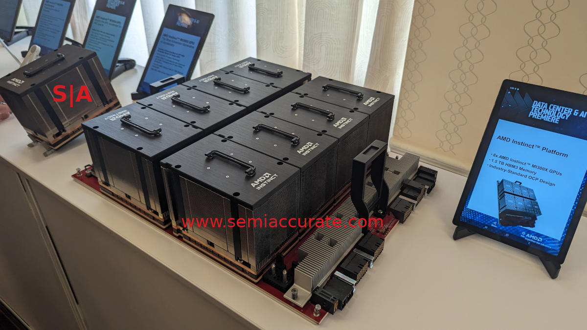
These are heavier than they look but eminently liftable
But wasn’t this article about an HBM Genoa, not GPU minutia? Well yes it was and it is, but the 8x MI300X vs 4x MI300A minutia is the backstory. Why not 8x MI300A? Because the MI300A system isn’t a bunch of GPUs on a PCB like Nvidia’s offerings, it is a full blown 1x Genoa system with 12x MI300-class GPUs on board. It is also a marvel of reuse and hints strongly at both the future of AMD consumer GPUs and a new component chiplet that we will probably be seeing a lot more of in the near future. Take a look at the following diagram.
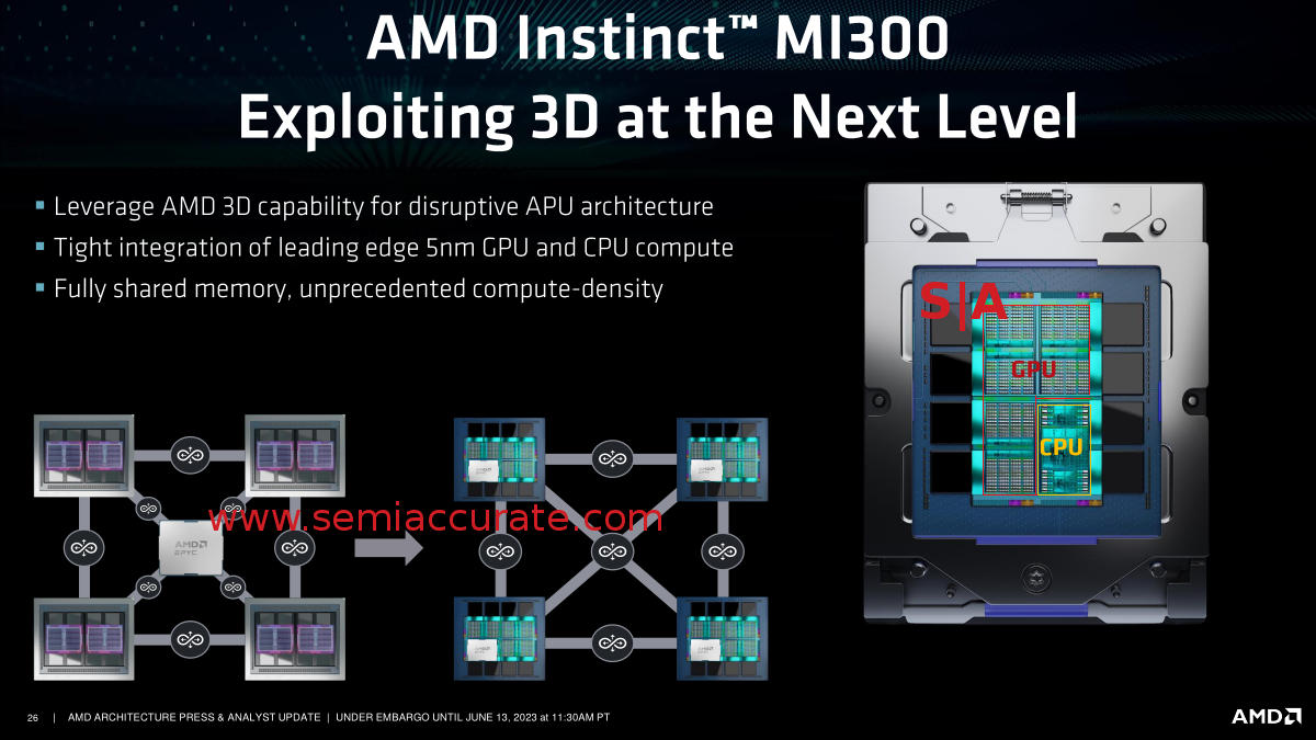
Five goes into four in the AMD world
Do recall that AMD’s interconnect between sockets is Hypertransport, a modernized version called Infinity-something depending on the marketing whims du jour, but it is still HT under the hood. Also recall that AMD’s interconnect between chiplets within a socket is also HT based, xGMI in market-speak but it is running HT/Infinitymumblemumble when you look closely. If you want more details, SemiAccurate wrote up HT/IF years ago, it has evolved but the fundamentals still remain. The take home here is that HT underpins just about every chip(let) to chip(let) connection AMD has. As they said in 2016, it is a physical layer agnostic protocol and the current product line is proof that they weren’t joking.
So if you look closely at the diagram on the left, you will see it has a Genoa CPU with lets assume 96C and 4x GPUs each of which has 4x GPU dies under the lid. There are also 8x HBM stacks per GPU, the same as in the MI300 package. This brings us to a total of 12 Genoa CPU dies, 1x Genoa DDR5 IOD, and 32x MI300 GPU dies/16x MI300 GPUs with 2-die each, along with their attendant 32 HBM stacks to make the system shown. What the specifics are on each chip/chiplet is irrelevant, we will just assume they are the same on both systems.
On the right we have the 4x MI300A GPU system which really downplays the whole idea of a CPU entirely. As mentioned above, each of the ‘GPUs’ has 3x Genoa CPU tiles/CCDs and 6x MI300 GPU tiles or 3x ‘full GPUs’. Across 4x MI300A’s, you have 12x Genoa CCDs which, wait for it, is a full 96C Genoa CPU. Imagine the coincidence, it must have floored an AMD engineer when they noticed that bit, eh?
Seriously though what AMD did is to take a full Genoa, split it into four parts, and spread it out into multiple packages. They could do this with relative ease because the protocol going between the CCDs on the same package is the protocol for going between sockets. Yes we realize timings are different and all of that, but if a 2x Genoa system is possible, this is exactly the same thing, just entirely different for everything but the protocols involved. Because those protocols are the only part that really matters, you can pull off a lot of tricks that seemed impossible in the recent past. Since the die size of 3x Genoa CCDs also seems to be exactly the same as 2x MI300 GPU tiles, you can mix and match those two units with ease. This is also how AMD was able to push out the MI300X ‘pure’ GPU with such speed when it became clear what the market actually wanted.
So with an MI300A system being a full Genoa with forcibly attached GPUs, what else is new? That pesky IOD we told you about is really the only important bit in the end. On a Genoa system, the IOD has all the DDR5 memory and HT/PCIe controllers on board, the CCDs are just CPU and cache plus a little plumbing. DDR5 is not HBM, nor are the two controllers interchangeable so a new IOD was needed. The MI300 line brought us just that, an HBM controller for the MI300 GPU line. And since the CPU CCDs fit in the same footprint, presumably have the same pad/pinouts, and so on, you can mix and match at will. Looking at the big picture, it is almost like someone planned this in advance.
So now we have a full Genoa IOD, in tile form, with HBM controllers and lots and lots of PCIe/HT lanes for good measure. Oh yeah, it is also 2.5D advanced packaging with the outside possibility of it being 3D, more when AMD officially talks. No we won’t hold our breath for a real technical briefing either, SIGH. The take home message here is AMD now has the ability to make a monster Genoa or more likely Turin device, Venice for sure. They can mix and match the same CCDs and GPU tiles between DDR5 and HBM IODs, PCB and interposer/stacked substrates, and possibly a lot more. They can also split up a CPU or GPU between sockets without (presumably) losing functionality or much performance. It is a true mix and match chiplet infrastructure at a level we haven’t seen before.
In the end, AMD literally just announced an HBM Genoa system. Sure it is only single socket and sure you have to buy 12x MI300 GPUs with it, but it is a true 96C HBM Genoa. And then in typical AMD fashion they downplayed it, botched the briefings, and wondered why they could only score one own goal at a time. Why AMD, why? That said the parts they tried really hard to downplay are significant and have impressive potential. Think Xilinx. Then think custom silicon from Hyperscalers. Then wonder why AMD can’t message anything to save their lives.S|A
Charlie Demerjian
Latest posts by Charlie Demerjian (see all)
- Qualcomm Is Cheating On Their Snapdragon X Elite/Pro Benchmarks - Apr 24, 2024
- What is Qualcomm’s Purwa/X Pro SoC? - Apr 19, 2024
- Intel Announces their NXE: 5000 High NA EUV Tool - Apr 18, 2024
- AMD outs MI300 plans… sort of - Apr 11, 2024
- Qualcomm is planning a lot of Nuvia/X-Elite announcements - Mar 25, 2024