 Intel is set to become the first company to mass produce non-planar transistors with their upcoming 22nm process. Others are talking about FD-SOI, FINFets, and several related structures, but only Intel is set to produce anything in the near future.
There has been a lot of talk about what Intel is doing, and a lot of incomplete or incorrect information put forward from many different sources. What Intel is making is called Tri-Gate transistors, something that is a radical departure from planar ‘2D’ transistors, and distinct from FINFets in a very important way.
To understand what the differences are, you have to look at the basic transistor architecture, and how they are made. The main idea of a transistor is simple, you have an electrical path that can be switched on and off via a third input. This potential to conduct or not conduct is the semi- part of semiconductor.
How that switching is achieved differs greatly between each company and process node. How that end result is made differs even more, and is usually the most closely guarded secret of any semiconductor company. Developing a new process node is probably the hardest and most expensive thing a semiconductor company can do, with R&D taking from years to over a decade. As things stand now, the cost of developing a new node and equipping a fab runs in to the billions of dollars.
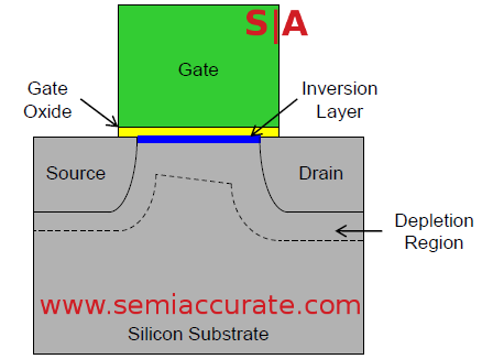
Planar transistor cross-section (Diagram courtesy of Intel)
The simplest type of transistor is a planar device, called 2D because it is flat. Flat is somewhat of a misnomer as you can see in the picture above, the gate stack does come up from the silicon substrate. The source and drain collectively called the channel, are where the electrons flow from and to. This channel is on the surface of the wafer, with the silicon itself connecting them, all of which is ‘2D’.
From there, there is a block called the gate on top of the channel, in green on the diagram above. The gate oxide, in yellow, prevents current flowing from the gate in to the current path itself. Theoretically, when you switch the transistor on, the electric field from the current in the gate extends down in to the silicon substrate. This modifies the electrical characteristics of the inversion layer allowing electrons to pass through.
One of the most common modifiers to the transistor is called PD-SOI or Partially Depleted Silicon Over Insulator. This attacks leakage, the phenomenon where current moves from the source to the drain when the transistor is off. Leakage is wasted energy, a very bad thing that is getting worse as transistors shrink. One way to combat leakage is to put a layer of oxide under the surface of the silicon to stop current from flowing below the gate, which explains the name quite nicely.
PD-SOI works well to a point, but the cost is not worth the benefit according to Intel. AMD has been using PD-SOI for several years, so they have a different view of the cost/benefit tradeoff. In any case, the benefits of SOI are largely a factor of the ratio between the source/drain channel and the depth of the oxide layer. As geometries are reduced, and structures shrink, the ratio needed means the layer needs to get closer and closer to the surface. Most companies are not using SOI below the 32nm node because of this phenomenon.
This leads to a new type of SOI called FD-SOI, or Fully Depleted SOI. In FD-SOI, the oxide layer is almost on the surface of the wafer, and all of the structures are basically built on that. One rule of thumb here is that the silicon body has to be thinner than the channel length, something currently measured in nm. Several companies have discussed making FD-SOI chips, but none have publicly committed to production. Cost and complexity are the two commonly discussed concerns, things that may or may not change before any FD-SOI chips come off the line in volume.
FINFets step from 2D to 3D (Diagram courtesy of Intel)
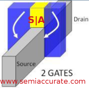
If you take a 2D transistor and flip it 90 degrees up, and then put another gate on the other side, you have a FINFet. The ‘fin’ is the source/drain channel, and you can make it as thin or as thick as you want. Instead of being the same thickness as the wafer, it is just another structure of the chip that you build up or etch down.
FINFets effectively have two coupled gates on either side of the channel, and a controllable channel thickness. The contact area between the gate and the channel is effectively 2x the size of a planar part, the channel is constrained on two sides, not one. This allows the electric field from the gates to penetrate the channel much more quickly and comprehensively. Because the speed and completeness of the field penetration through the body controls the speed of the transistor and the ramp of the on/off curve, more penetration means more performance.
FINFets allow much more room for tradeoffs in power and performance. These new knobs for the chip designer to turn means more control over some previously static parameters. More importantly, there is a huge reduction in area between the channel and the silicon substrate. If you recall, a lot of leakage is a result of current flowing under the gate, so if you reduce the gate to channel contact area, you reduce leakage a lot.
The biggest problem with FINFets is not conceptual, it is physical. How do you make them? Instead of laying down layers of materials or implanting ions on the surface of a flat wafer, you have to make a set of extremely thick but narrow high aspect ratio structures. Instead of painting on a canvas, FINFets force you to stack bits of colored atoms on edge to achieve the same picture.
The problems are immense and most of them involve how to make high aspect ratio structure with effectively flat, right angle walls. Since the performance of the transistor is related to the thickness of the fin, any variance in widths, typically the top thinner than the bottom, means inconsistent performance and a host of other problems. Making correct and consistent structures by the billions is extremely complex work.
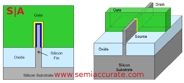
Tri-Gates from two directions (Picture courtesy of Intel)
Confining the channel on two sides with FINFets is good, but wouldn’t three sides be better? If you look at the FINFet pictured above, you will see a cap on top of the fin meaning no gate contact on the third side. With their 22nm process, Intel added gate contact on the third side, instead of a cap, they put more gate on top. This increases manufacturing complexity a bit, but it also constrains the channel on a third side, leading to the tri- in Tri-Gate.
According to Intel, Tri-Gate performs better than FINFets in a few cases, and no worse in all cases. It is another tradeoff, and one Intel seems to think is well worth the cost for their 22nm process. The end result is a claimed 37% performance increase at low voltages or 50%+ lower power use at the same performance. These macro level gains are the result of the reduced leakage, faster switching, three sided confinement, and increased drive strength inherent in the vertical ‘3D’ fin structures.
One interesting thing about FINFets and Tri-Gate transistors is the area reduction, and ability to parallelize transistors for increased drive strength. Instead of tuning the transistor by varying thicknesses of layers, a designer can simply put a second channel beside the first. Or a third beside that, and as many more as you want to draw if you need to do silly things like ESD protection on I/O circuitry.
The end result is that some of the tuning available to Tri-Gate transistors is now quantized. Instead of tuning an analog radio, you have a knob with specific stops. You can still tune the vertical fins in some of the same ways as planar, but that route is much harder than before. The net result is a few different tuning parameters than before, but things are still quite tunable. Think about there being some new knobs, some old knobs, some missing knobs, and some different knobs, but there are still knobs. That is the important part.
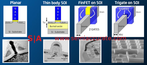
Planar to Tri-Gate progression (Picture courtesy of Intel)
As mentioned earlier, Intel is the only one currently slated to produce non-2D chips in the near future. Other companies have talked about FINFets, but none are talking about Tri-Gates yet, and all of those conversations tend to center on problems, not production plans. The theory behind Tri-Gate is sound, production plans are in place, and the end results will be known in early 2012 when the first 22nm Intel CPU family, code named Ivy Bridge, comes out.S|A
Charlie Demerjian
Latest posts by Charlie Demerjian (see all)
- Qualcomm Is Cheating On Their Snapdragon X Elite/Pro Benchmarks - Apr 24, 2024
- What is Qualcomm’s Purwa/X Pro SoC? - Apr 19, 2024
- Intel Announces their NXE: 5000 High NA EUV Tool - Apr 18, 2024
- AMD outs MI300 plans… sort of - Apr 11, 2024
- Qualcomm is planning a lot of Nuvia/X-Elite announcements - Mar 25, 2024


