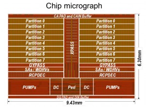
Samsung unveiled the first 20nm PRAM part at ISSCC in San Francisco last week. The density still lacks behind NAND flash as the chip capacity is 8Gb compared to 128Gb for the most advanced NAND flash chips.
However, the chip does have some distinct advantages. First of all it uses a much simpler design with fewer process steps, which potentially makes it cheaper to manufacture at high volumes.
It also has a much better endurance as it can tolerate hundreds of thousands of writes compared to flash that has a tendency to wear out after less than 10,000 writes.
Add to this that the chip is bit addressable and has a bandwidth of 40MB/s and is compatible with NOR flash.
This makes the chip a potential candidate for hybrid memory systems in the initial phase, but could eventually lead to memory system based solely on PRAM.
Samsung does, however, warn that care should be taken because of the high voltages up to 1.8V involved when designing for the chip. The new chip was just one of many new and existing memory technologies shown off at this year’s ISSCC.S|A
Mads Ølholm
Latest posts by Mads Ølholm (see all)
- Samsung shows off 20nm PRAM - Feb 28, 2012
- DDR4 shows up in the wild - Feb 28, 2012
- SanDisk develops the world’s smallest 128Gb flash chip - Feb 22, 2012
- Aussies create single atom transistor with precise control - Feb 21, 2012
- Chinese 16 core CPU uses message passing - Feb 21, 2012
