 One of the questions that has been bothering process geeks for months now is how Intel is doing Vt control in fin structures. While it is obvious they can do it, 22nm chips are out in volume, the particulars and limits were still an open question.
Luckily, Intel today put out a paper at EIDM on that topic, and it laid out most of what we didn’t know. The authors went in to detail on how Intel differentiates between high power, low power, and high performance transistor, plus a little detail was given on passive devices, memory, and analog structures. In short, if there were lingering questions about the edges of what is possible, they are mostly gone now.
The big concern that SemiAccurate had was that Vt control would be problematic on a FinFET. Ion implant is extremely tough with high aspect ratio structures, and the obvious method of the past, changing contacted gate area by making the fin taller, is a non-starter. Why? If you make transistors at an uneven height, it makes the next few layers a bit tricky, usually fatally so. The other way to increase contacted area, making the gate longer, eats die area, removes the additional benefits of going vertical. While added length works, it has a high cost, and somewhat defeats the purpose of using the third dimension.
The numbers that matter
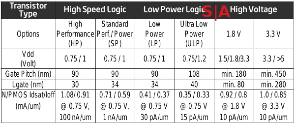
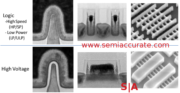
In the end, there was no magic, Intel did the obvious and made the transistors different lengths. There are two things to note in the table above, gate pitch and gate length. Compare and contrast that to the Vt and it becomes pretty clear that length is the overriding factor for Vt control in Intel 22nm transistors. Pitch also varies quite a bit, but you need to make structures thicker if you run more energy through them, and pitch is where it plays out. Take a look at the electron micrographs below for a look at the transistors themselves.
Through gate on the left, side view middle, and top view on the right
There are two things of interest here, first is the length difference between the high and low voltage transistors. Notice that the high voltage transistor is longer than two discrete low voltage parts and the interconnect between them. Higher voltage comes at a fairly steep price, and vertical transistors don’t help much here, they might even add some cost.
The other thing is much more subtle, but you can see it in the cross section on the left, there is an extra layer between the channel and the gate. This layer supports higher power, it is a ‘hybrid’ dielectric that adds silicon dioxide to the normal High-K gate material. With this Intel can scale the voltages to 5v and beyond. This should be enough, most modern I/O doesn’t come close to 5v, at least for anything connected to the CPU.
Metal layer table and pictures
From there, the interconnects also bring some new twists. On Intel’s 22nm process, you can use between 8 and 11 dielectric layers, Low-K or UltraLow-K, mix and match. The ULK layer is Carbon Doped Oxide (CDO), the Low-K material is not specified. Intel uses self-aligned vias, sacrificial hard masks, and and double patterning on M1. The rest of the layers all are single patterned. What is chosen, and how many are actually used depends on the process, CPU or SoC, and the exact project.
Intel doesn’t stop there, to make a chip you need passive components, memory, and possibly a bit of analog here and there too. Intel has shown off spiral inductors, very high precision resistors with <15% variance, and three capacitor types. In addition to the standard and metal finger caps, Intel has a new high density structure they call MIMCAP. As an aside, this is not where that glowy bit from the Roswell pictures ended up, that isn’t productized until 14nm unless you are a military buyer.
For memory, Intel has described high density, low voltage, and high performance single ported memory. In addition, they also have dual ported SRAMs in both synchronous and asynchronous flavors. Between these types and the passive devices, Intel can support just about any type of SoC it wants to, and that is the idea.
When 22nm first came out, there were a lot of theories about it from those who didn’t really understand the tech. It wasn’t helped by Intel’s reluctance to talk about anything but marketing fluff, but the tech eventually came out. Some questions were not answered though, most notably around the SoC process and Vt control. Intel either needed to do some magic, or simply to eat planar area to get to where they had to be. In the end, it wasn’t magic, just good engineering and added area, but they got to the desired end point. It looks like Intel has a 22nm process that can do just about everything needed for a modern CPU or SoC, and that was the goal to begin with.S|A
Charlie Demerjian
Latest posts by Charlie Demerjian (see all)
- Qualcomm Is Cheating On Their Snapdragon X Elite/Pro Benchmarks - Apr 24, 2024
- What is Qualcomm’s Purwa/X Pro SoC? - Apr 19, 2024
- Intel Announces their NXE: 5000 High NA EUV Tool - Apr 18, 2024
- AMD outs MI300 plans… sort of - Apr 11, 2024
- Qualcomm is planning a lot of Nuvia/X-Elite announcements - Mar 25, 2024


