![]() At the Common Platform conference today, IBM showed off a bunch of goodies including two new types of wafers. Of the two, the 14nm wafer was expected, the flexible wafer was not.
At the Common Platform conference today, IBM showed off a bunch of goodies including two new types of wafers. Of the two, the 14nm wafer was expected, the flexible wafer was not.
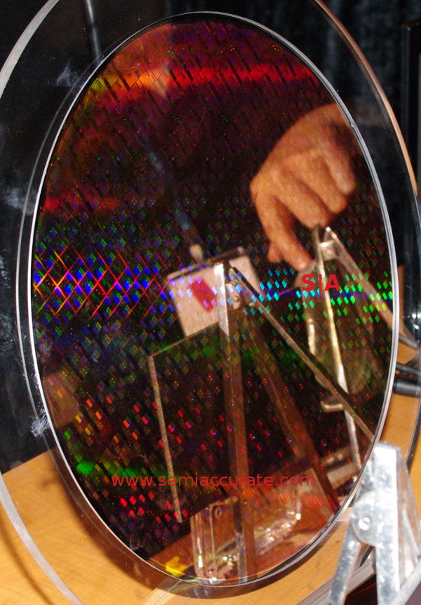
14nm wafers are here
The 14nm wafer is just that, 14nm FinFETs with 20nm everything else, so it is a true 14nm-ish process. These are just test chips but as you can see, it is real. If you squint, you can see that each transistor has very little variability too, but unlike 20nm, it is a little more subtle to the untrained eye. Yes, that is a joke, you need a magnifying glass. Yeah, that was another joke.
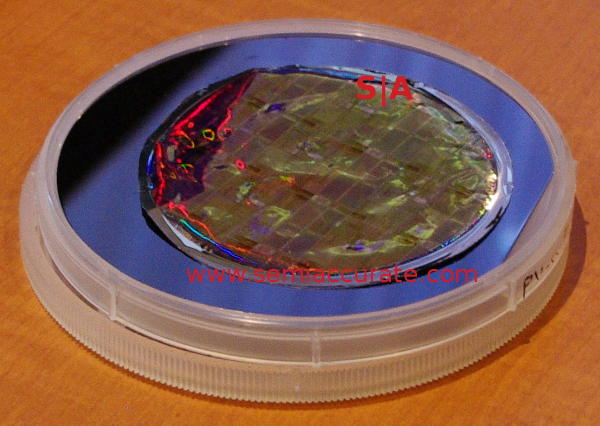
Bendy wafers for bendy devices
The next one up was a little more unexpected, a completely flexible wafer. It is a 6″ test device, but the transistors are very resistant to physical strain and show little performance variance when bent quite a bit. These devices are built on a 28nm FD-SOI wafer with an embedded fracture plane. Once the device is made, you fracture it, and the silicon left is both thick enough to keep the transistors in place, but thin enough to be rolled in to the diameter of a dime. And yes, it still works. Neat.S|A
Charlie Demerjian
Latest posts by Charlie Demerjian (see all)
- Qualcomm Is Cheating On Their Snapdragon X Elite/Pro Benchmarks - Apr 24, 2024
- What is Qualcomm’s Purwa/X Pro SoC? - Apr 19, 2024
- Intel Announces their NXE: 5000 High NA EUV Tool - Apr 18, 2024
- AMD outs MI300 plans… sort of - Apr 11, 2024
- Qualcomm is planning a lot of Nuvia/X-Elite announcements - Mar 25, 2024