(Editor’s note: Part 1 can be found here.)
The next premise in the note is that 22nm is having scaling problems, and 14nm will suffer or be delayed as a result. This is due to the process needing significant modifications to scale down to the next node. Stepping back from the strictly technical explanation, about the best explanation we can point to for large changes between 22nm and 14nm is, “Well duh!”.
Intel process changes from 90nm to 22nm
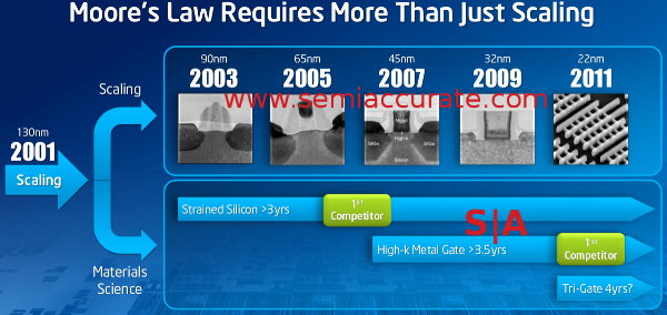
To step back into technical mode, lets look at the Intel processes of the past using P12 of Brian Krzanich’s slides from the recent Intel Analyst Day.
Moving from 130nm to 90nm, Intel introduced Strained Silicon, a fundamental change in chemistry, process, and physics relating to how the transistor works on a basic level. This is a massive change in materials and manufacturing, not to mention adding an entire new property to the physics of the device. Strain engineering is not at all trivial. 65nm introduced what is called ‘second generation strain’, again, a completely new set of materials that work in a very different way, but end up with the same type of result. It is totally different in many key ways to first generation strain.
You could conceptualize this similarly to going from one type of FinFET/TriGate to another, before you had strained silicon and after you had strained silicon, with totally different everything but the name. Now you have TriGate and on 14nm you will have TriGate, but like 90nm to 65nm, they are completely different in everything but the name. Going from 130nm to 90nm was a complete change, 90nm to 65nm was a complete change, and that was par for the course a decade ago.
65nm to 45nm brought in High-K Metal Gate (HKMG) technology, and that moves the gate itself from silicon to Hafnium. Silicon is not metal, Hafnium is, hence the metal gate nomenclature. Since Gordon Teal invented the first Silicon transistor in 1954, the gate has been made out of silicon. Intel’s 45nm process changed that to Hafnium. Can you get a more fundamental change than that for the 65nm to 45nm transition? I can’t think of how you would.
45nm to 32nm was a bit more minor, but still fundamental change to the process with their second generation HKMG process. It added quite a lot, most notably strain was added to parts of the device where there was not strain available at 45nm. It may seem trivial, but the chemistry changes were once again completely fundamental, similar to the 90nm to 65nm shift. It was not a simple shrink by any stretch of the imagination.
32nm to 22nm saw a similar shift in process tech, from a planar (flat) structure to a vertical ‘3D’ gate. This is a FinFET, and Intel calls it TriGate, but the idea is to take what was formerly in-plane with the wafer, and have it jut out of the wafer vertically. You can read all about it here if you want the technical explanation.
So, fundamental changes between 130nm, 90nm, 65nm, 45nm, 32nm, and 22nm, with the 90nm to 65nm and 45nm to 32nm shrinks being harder to explain without an accompanying PhD thesis. Even if you discount those two shrinks as being ‘fundamental’, that still leaves four of the last six shrinks having unquestionably fundamental changes needed to produce them. If the 22nm “process likely needs significant modification to scale 14nm”, all we can say is ‘Duh’.
The next premise needs a little background information, Intel uses a separate low power variant of its processes for the Atom chips, and these are usually introduced far later than the non-low power process. How much later? 32nm was introduced in Q4/2009, the first 32nm Atom, on the low power process, was introduced in December of 2011, six months ago.
Intel says it came out in Q3 of 2011, but it was delayed and delayed and delayed, not for process reasons, but because it stunk.
Intel kept Atoms on 45nm until 22nm was about to be released for mainstream parts. This was more for internal political reasons than any mythical process tech problems, but since we don’t kiss and tell, all we will say is look to executive changes in the ultramobile space for hints.
This brings us back to the note in question, and its premise that “22nm SoC process for mobile will be extremely challenging/expensive”. Other than the fact that any process development effort on modern nodes costs hundreds of millions of dollars on a good day to billions on a bad one, the expensive part isn’t in question. The fact that Intel is bothering at all says they have a good business case to do so, the company is not in the habit of wasting money on fools errands. *COUGH* Itanium *COUGH*. Ok, maybe they are, but this process does make technical and financial sense, the hard work was done and paid for by the mainstream 32nm. 32nm low power is cheap by comparison.
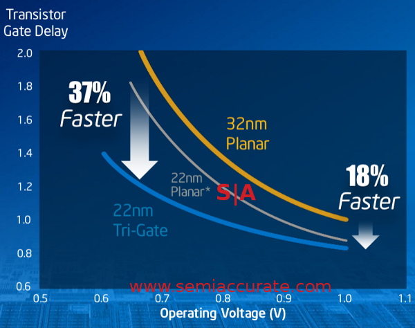
Speed vs Power curve (slide 10)
The idea for a low power (LP) process is that you take the traditional speed vs power curve, and use a different part of it. Gate delay in the picture above is just what it sounds like, how long it takes for each transistor to change state and switch. The 32nm device listed above takes ‘2’ time units to switch at .7v or ‘1’ time unit to switch at 1v. Since energy used is proportional to the square of voltage, that means switching in half the time takes ((.7*.7)/(1*1) = .49) about half the power.
For an SoC/LP process, Intel takes the existing 32nm process, and makes transistors on the slower and lower power side of the curve. If you want to customize the process, one way to do it is to make the gate thicker and the transistors larger. Vastly simplified, this minimizes leakage, and allows more complete switching. The key point to remember is that you make things bigger and thicker for lower power.
Developing this LP process costs a lot of money, not because it is harder and tolerances tighter, but because there is a lot of work to do in figuring out what to make, how thick to make things, and how you can most efficiently get your desired results. The curve above is for one set of transistors, if you make them at different sizes, you need to plot out the curve, test, verify functionality, and hundreds of other details. It takes time and effort, and that is where the money comes in.
On the technical side however, it is, if anything, easier to make than the ‘fast’ process. Why? The transistors are bigger, and bigger is easier to make than smaller. If you can make a device with 32nm design rules, adding 10% to many, if not all of the dimensions is roughly the equivalent of 35nm design rules. This is not a challenge if you have been making 32nm at high yields for over a year.
Moving back to 22nm, that process is simply not proving difficult for Intel at the present time, so a 22nm LP process may be not easy or quick to characterize, but it is an easier problem than making 22nm transistors from scratch. SemiAccurate does not see any problem with Intel developing a 22nm SoC process, quite the contrary.
Why? Instead of a late 2013 introduction, as would be expected for a 2 year process cadence step from the Q4/2011 32nm-LP launch, Intel is planning on showing 22nm Atoms next January.
Instead of a Q1/2015 launch for the 14nm-LP Atoms, Intel has privately committed to a Q1/2014 launch, a year after 22nm-LP Atoms. This means 22nm-LP is a year earlier than scheduled, and 14nm-LP is currently set to launch before 14nm non-LP. While neither is out yet, those roadmap pull-ins do not signify a bug-ridden and problematic development process.S|A
Charlie Demerjian
Latest posts by Charlie Demerjian (see all)
- Qualcomm Is Cheating On Their Snapdragon X Elite/Pro Benchmarks - Apr 24, 2024
- What is Qualcomm’s Purwa/X Pro SoC? - Apr 19, 2024
- Intel Announces their NXE: 5000 High NA EUV Tool - Apr 18, 2024
- AMD outs MI300 plans… sort of - Apr 11, 2024
- Qualcomm is planning a lot of Nuvia/X-Elite announcements - Mar 25, 2024

