![]() At Hot Chips this year, Xilinx gave a good talk on the problems with electrical and optical backplanes, and what the options are to deal with some thorny impending problems. Nothing was given as an overarching solution, the speaker just called out the pain points that we are heading towards, and some options to deal with them.
At Hot Chips this year, Xilinx gave a good talk on the problems with electrical and optical backplanes, and what the options are to deal with some thorny impending problems. Nothing was given as an overarching solution, the speaker just called out the pain points that we are heading towards, and some options to deal with them.
The first problem is simple, electrical data transmission is bounded by a very simple line on a distance vs rate graph. As you can see below, the number ends up being about 100Gbps per meter, the longer you go the lower the throughput. According to the talk, the formula here is not just theoretical, there are reams of data to back it up.
The graph that underlies the problem
If you want more throughput between your devices, you need to use more wires, shorten their length, or both. Obviously, these have practical limits, you might recall the whole issue of chips becoming pin bound a few years ago. This issue lead to serial buses instead of parallel, not to mention flip chip packaging, and other related connection density advances. These solutions, and the impending stacking revolution only buy the industry time, but the end of practical increases in electrical throughput is becoming clear. The only real solution long term is to go optical, and that brings on a whole new set of problems.
The simplest backplane is a passive electrical one, think about two cards in slots like PCIe that are just wired to each other, no chips between them. The only thing between the slots are traces, the backplane is just a physical connector and wires. The cards that plug in to the backplane also only have wires to the chip that does the communication, it is completely passive otherwise.
Stepping up to the next level, imagine if you put a device on the traces to boost the signal strength, clean the signal, or both. This could be on the backplane, but is usually on the cards that plug in to them. You would probably need one on each end as well, so the complexity goes up, and so does the effective throughput. Countering this happy ending is the dual problems of added latency and increasing costs. This solution currently works, but it is what we meant when talking about the impending limits to scaling, it won’t keep advancing much longer.
So what do you do? You go optical, not because it is cheaper, but because you can’t achieve the transmission rates you want any other way. If you want greater speeds, lower latencies, and the ability to get more throughput than an electrical solution can deliver overall, there is no other way. But that brings up the thorny question of exactly how you do it. Electrical connections have some pretty well defined interfaces, optical anything is nowhere near ready yet.
The most obvious one is easy enough, you take the active electrical links above and replace the signal boosting devices with Electro-Optical converters (EO or OE) and replace the wires with waveguides. This is nice, and it works well but wouldn’t it be better to just put the optical bits on the chip itself? That would bring you back to the happy days of passive backplanes, just dumb traces or in the case of optical, dumb waveguides.
With either solution, the first problem is how do you physically connect the wires, waveguides, or both? Who sets the standards? Will it be cheaper to put the EO/OE bits on the cards or on the package? If you were reading the above parts about electrical scaling, you might be thinking that going to optical on the card will buy us a generation, but the chips themselves will soon become pin bound. All you are effectively doing with this solution shortening the electrical trace to the distance between the chip and the card. That will buy you some time, but the 100Gbps/M rule will still bite you just as hard because those chips can only get so close.
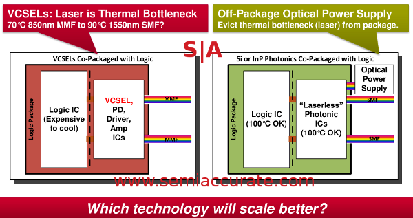
Obviously, the solution is to put the optics directly on the chips, bandwidth to the EO conversion hardware is effectively infinite, at least for the time being. So you put the lasers and optical modulators on the chip and all is happy again, right? Well not quite, there is this little problem of heat, take a look at the two options below for more.
Optical packages with and without lasers, both without sharks
Notice the problem? Lasers are fairly heat sensitive, their frequency varies quite a bit with the temperature. Chips can get hot, going from room temperature to 100C in very short periods, but with a decent heat sink and fan, as long as things are within specified ranges, there is no problem. Laser light sources also generate quite a bit of heat, and their temperature needs to be controlled much more precisely than standard semiconductors or you get some intolerable frequency shifts. The solution? Control the temperature very carefully.
If you put the laser on the chip, or more likely on the package, you have to remove not only the heat generated by the laser, but also that produced by the IC attached to it as well, and keep them both in a tight range. This is unnecessary for the semiconductor, as long as you are within their fairly wide window of operating temperatures it really makes no difference, doing it is expensive and consumes quite a bit of energy.
The solution is to separate the laser source from the semiconductor package so you only need to control the temperature of a much smaller heat source precisely, the larger one can be left to vary more. This solution is not just cheaper, but it is also more energy efficient and likely more stable across a wider range of ambient conditions. The optical portions of the chip only need to modulate the optical signal, not generate it, so they are as temperature insensitive as the semiconductors. Unfortunately, there are no standards, connectors, or really even consensus on how to go about doing this yet, so it is going to be quite proprietary at first.
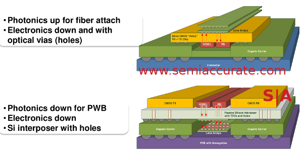
That brings us to the next problem, assuming you are going to put the photonic bits, other than the laser itself on package, how exactly do you do it? VCSEL stands for Vertical Cavity Surface Emitting Laser, and it means what it says, the light goes straight up. This is good in some ways, but bad in others, stacking them being an obvious negative. Other laser types require different mounting solutions that have other problems and benefits. So how do you do it in practice?
Sunny side up or down?
Once again, there are multiple ways and no real consensus yet, if there ever will be. If you point the lasers up, you can attach the fibers on top of the stack quite easily, but the lasers are down in the stack where it is hotter. If you put the lasers on top where they are cooler, the fibers are in the middle of the sandwich where it is a bit trickier to align and attach them. Either way, the signal must be routed through the interposer, something that can finally be done with recent advances in POVs (Passive Optical Vias aka holes punched in the damn thing).
Both methods have their own unique set of problems, costs, and benefits. One thing for sure is that there is no single solution, no one set of rules to pick a solution for a given problem, and very few companies making components and tools. Few companies have the skill sets to assemble disparate pieces given to them, and the lack of standards doesn’t make things easier either. It is the wild west at the moment.
Luckily, companies like Xilinx are taking the entire chain of problems, solutions, and costs quite seriously, and they are not at the electrical wall yet. Some things are more promising than others, and there is work going on to define various standards as well. Other companies are making tools, OSATs are figuring out how to assemble things, and progress is again being on all fronts. While the entire industry is nowhere near ready for the optical interconnect revolution, no one seems to be idly sitting by hoping someone else figures it out before their own needs are critical. In the end, that is quite hopeful, and no one seems to think we won’t get there in eventually.S|A
Charlie Demerjian
Latest posts by Charlie Demerjian (see all)
- Qualcomm Is Cheating On Their Snapdragon X Elite/Pro Benchmarks - Apr 24, 2024
- What is Qualcomm’s Purwa/X Pro SoC? - Apr 19, 2024
- Intel Announces their NXE: 5000 High NA EUV Tool - Apr 18, 2024
- AMD outs MI300 plans… sort of - Apr 11, 2024
- Qualcomm is planning a lot of Nuvia/X-Elite announcements - Mar 25, 2024


