![]() Today Intel is talking about all things process, construction, and foundry in more detail than before. SemiAccurate has weighed in on some of these things in the recent past, now it is time for the next big reveal.
Today Intel is talking about all things process, construction, and foundry in more detail than before. SemiAccurate has weighed in on some of these things in the recent past, now it is time for the next big reveal.
Background:
Lets point out the elephant in the room right off to save us all a lot of caveats later in the story. Intel’s process developments for the past 5++ years, yes that is a backhanded joke, has been a mess. Their public proclamations have been technically correct on some level but more often than not intended to mislead, some have even been what SemiAccurate considers outright lies but there was likely something lurking beneath the covers to pass muster with legal. In any case their credibility is well below zero when it comes to anything process or fab related.
That was the old Intel, this is the new Intel and it is really trying to be different from the top down. There are some new faces, some new old faces, and a lot of old old faces but things are definitely changing. That said at this point Intel can talk all they want but they will only start digging out of the very deep hole they are in when they prove it. Since nothing in the process and fabrication world is quick, this may take years.
What we are trying to say is anything Intel says at this point should be taken with a grain of salt, a very very big grain. SemiAccurate is cautiously optimistic that things are indeed moving in the right direction, the old messaging paradigms look to be disappearing quickly and given top management, are unlikely to reappear. For the rest of this article we won’t keep putting caveats on every one of their claims, just know we are not taking them at face value until there is proof. Enough with the disclaimers, on with the show.
Foundry 2.0 or is it 3.0?:
Intel is making another attempt at being a foundry, this time in March at an event called Unleashed. There are talks of many more fabs, SemiAccurate exclusively revealed the numbers on US and EU incentives, and even overhyped claims of buying GlobalFoundries. In short this is not a small undertaking, each fab is in the $10 billion range so a handful more starts adding up to real money quickly.
This investment would be taken better if not for Intel’s woeful track record on both process development and as a customer foundry. Intel is now 2 full nodes behind the competition, give or take, and if they want to have any realistic hope of return on their investment, they need to close that gap. More on this later but spending tens of billions of dollars on products that are nodes behind the competition won’t end well.
Worse yet is their history as a foundry. If you go back through the list of previous customers you see names like Cisco, Panasonic, LG, Nokia, Ericsson, and Altera alongside several small, almost captive customers. Most of the names listed never came out with a chip and were keen to pretend the relationship never existed. LG had their entire SoC efforts killed by Intel’s 10nm problems and enough money changed hands in the aftermath to make sure LG never publicly complained. In any case it had a huge price tag and a gutting effect on LG’s silicon efforts.
That was bad but it pales in comparison to the next set of victims, Nokia, Ericsson, and other 5G infrastructure silicon customers. Intel’s foundry mess singlehandedly delayed the introduction of 5G in many parts of the world and cost the partners billions of dollars. SemiAccurate reported the Ericsson side of things here, and lest you think we are joking, take a look at the dire bits in Ericsson’s financial statements. (Authors Note: If you haven’t read this link, you really should, it is mind-blowing.)
Other were similarly affected but not as public about the problems. Intel again had to paper this over at huge expense both directly and indirectly. The net result was massive losses everywhere, most of which were unlikely to be covered by the ‘generous handouts’. If you want to see the most significant long term fallout, look at Samsung’s share of the 5G infrastructure market during the last 4 or so years, they don’t use products based on Intel’s 10nm silicon. It isn’t pretty. Also look at the throughput on 5G networks using Intel silicon vs Samsung vs Huawei, again a stark contrast.
In light of this and several other huge and expensive flameouts, Intel has a long way to go with any foundry efforts. Things may have changed radically but would you base your critical infrastructure on that? If you are even thinking yes, ask LG how it turned out for them, that division is literally gone. Intel can make headway and prove their value but to get real customers, SemiAccurate feels they will need to prove their process development is on track, reliable, closer to the current state of the art, cost effective, and offers things no one else does. About that…
The Roadmap Gets Smaller:
One key thing Intel promised at the Unleashed event in March was a yearly cadence on new process releases. This can be read two ways, one good one bad. The bad is simple, most foundries are also on a yearly cadence with a new node every two years and a half-node in the intervening years. examples of this would be a 14nm node followed by a 12nm half-node, 10nm node followed by an 8nm half, 7/6nm etc etc. That is normal and if this is what Intel means by yearly, they will never catch up.
On the brighter side if Intel does a full node every year as was intoned at Unleashed, they could catch up in four years and be credible in less time. While we won’t get into the details of how they could do this many full steps in half the expected time, lets just say there is a credible path for them to do so. If all goes according to plan, things will look like this.
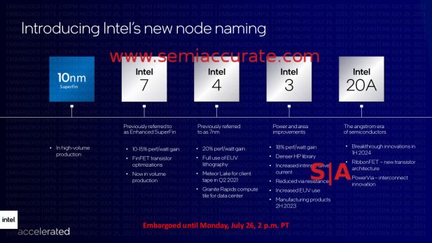
The New Intel Process Roadmap
There is a lot to take in on this slide, some good some bad. OK some good some shatteringly stupid but the end result is a good place with a few holes dug between now and then. We will also assume that these steps are on a more or less yearly cadence. If so Intel will catch up to TSMC a little past the edge of the roadmap above, probably the node past 18A. This assumes Intel does execute correctly on their plans, something we feel is possible at this point, and TSMC doesn’t pull something out of the bag which is also possible but less probable. That said lets take a look at what Intel is planning.
Stupid Stupid Stupid Stupid:
Just when you thought the digging stops, Intel digs faster, pulls out the footgun, fires twice, then resumes digging. If you don’t get the intonations here, we are not a fan of the first step of this roadmap, the ‘7nm’ node. Why? Because it isn’t 7nm, it is 10+++, the process formerly known as Prince, I mean SuperFin+. The tenuous technical claim here is that Intel’s nodes are equivalent to one node ‘better’ by the foundries, IE foundry 14nm ~= Intel 22nm, foundry 7nm ~= Intel 10nm etc etc.
This is a valid claim and one borne of underhanded marketing by the foundries but that is the past. While we understand why this bothers Intel and why they would want to do something about it, doing so is fraught with problems. SemiAccurate went into the issue here and we feel Intel is playing a really stupid game that they can’t win. Obviously no one learned from the Ultrabook mess which they claimed would allow low budget OEMs to ‘out-fashion’ Apple. Guess who won that battle? Guess who will win this one?
While the renaming of a 10nm variant to 7nm has some technical validity, doing so now is abjectly stupid and will poison the rest of Intel’s much more valid naming moves. ‘7nm’ was 10+++/SuperFin+, and that naming was quite well understood and accepted. Arbitrarily deciding to change the name halfway through a node smacks of marketing desperation and strongly intones there is a lack of technical merit underlying the move. This is in fact the case.
It is an own goal of spectacular proportions that didn’t need to be done, there is literally no upside and massive non-theoretical downsides like SemiAccurate questioning the intelligence of anyone involved in this debacle. The marketers at TSMC and Samsung are going to have a field day with this. It instantly poisons everything else on the roadmap, 4nm, 3nm, and the Angstrom branding. Instead of a clean new start everyone is going to question everything for the next few years. Like we said, stupid stupid stupid stupid. There is no tech that justifies this move, period.
4nm and 3nm:
Moving on to the next two nodes, there is justification to rename 7nm to 4nm and 5nm to 3nm. This move is simply bringing it in line with the foundry naming flows but it does two things wrong. First it says Intel is behind, knows it, and is chasing with marketing rather than tech. This may or may not end up being true but it sure looks bad. Second while it takes a few liberties with the numbers but SemiAccurate feels there is enough justification to not be that far out of line. Intel’s old 7nm was better than TSMC’s 5nm but enough to call it 4nm? If not for the 10+++ -> 7nm debacle we would cut Intel some slack but now we have to question it. Same with the new 4nm -> 3nm transition, it seems more like a half-node than a full node, wouldn’t 5nm -> 3nm have been more impactful? The overly optimistic naming at a time when Intel has used such overoptimism illegitimately for years is not a good look, a little more humble and less hubris would go a long way right now.
In any case 4nm is not the old 7nm, it uses much more EUV as Intel has previously spelled out and is likely a significantly different and better process than the pre-Pat 7nm. Intel claims their Meteor Lake CPU on 4nm has taped out but that is a long long way from volume production at viable yields. Same of parts of Granite Rapids, a chip we don’t expect until 2024, are also on this process but weren’t specified to be taped out like Meteor Lake.
SemiAccurate thinks that 4nm is indeed doable by mid-2023 if all goes well so take that as a starting point for the yearly cadence. ‘7nm’ is said to be in volume production now, not a stretch since it is a mild 10nm variant, so a hard yearly cadence looks a little tenuous at the moment. Intel is claiming production in late ’22 but that probably means no products on the market until 1H/23 and volume in mid-23.
20A is a New Convention:
Neither the new 4nm or 3nm variants look to have any big bang techs other than increased use of EUV and a lot of advanced packaging on the product side, more on that later. From a technical perspective the goodies all come with the 20A process. First a bit on the naming, 20A is for 20 Angstrom, an attempt to get back to the crazy notion of process names being tied to physical structures. It could very well be a solid naming scheme, time will tell, but the concept is good so far.
SemiAccurate had two thoughts on this new direction, the trailing -A makes it seem a bit like a variant of 20, IE 20A, 20B, 20C rather than 20 Angstrom. That said A20 et al is likely to stop the flow of chirpy holiday cards from Cupertino and replace them with slightly nastier letters from lower creatures like lawyers. We get this but… but… we can’t think of much that would be better other than 20Au, that would be golden. Sorry had to.
The biggest problem with Intel’s naming releases today are at the beginning and end of the line. 10+++ -> 7nm was idiotic, unjustified, and damaging to their already wounded reputation. 20A is the way of the future and makes a lot of sense. Why rename one process to a different type, SuperFin to number, then go back to normal nanometer numbers, then go to Angstroms? If Intel had renamed everything Angstroms out of the gate, 10+++/SuperFin+ -> 70A, 7nm -> 40A, etc etc, problem solved. No one would complain, no damage done, no roadmap changes poisoned for years to come, and no deliveries of ammo to competing marketing teams. It would have made technical sense, been a clean start, and off you go. Instead we have three naming changes in one roadmap and only one is justified. Why?
The Tech:
In any case there are two big bangs that come on the 20A process, RibbonFET and PowerVia, both are significant improvements. You might notice that the claim is for 20A to be in production in 1H/24 so with PowerVia being 2024 sans 1H. So this likely means there are several 20A variants during that year rather than 18A coming in 2024. So what do these things do?
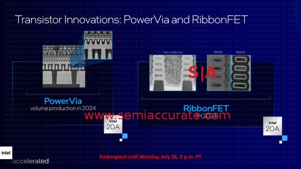
PowerVia and RibbonFET technologies
PowerVia is essentially backside power delivery through, wait for it, vias. This allows Intel to deliver more power directly to the transistors and lower layers while freeing up the higher layers for routing. While we won’t go into the tech here, just be aware there are a lot of waterfalling benefits from PowerVia in routing, metal layer thickness, and more. In short PowerVia is a really good thing if done right.
RibbonFET is Intel’s name for GAA or Gate All Around transistors. Like TriGate was a branded FinFET, RibbonFET/GAA is an industry wide move that essentially has to happen if progress on transistor performance is going to be made. Both TSMC and Samsung have GAA nodes on the roadmap and TSMC is likely to get there before Intel even with the new accelerated roadmap. There really aren’t any details at the moment on how if at all RibbonFET differs from the generic GAA transistors so stay tuned. This is a big leap in transistor performance, the only question is who jumps further and when, the others aren’t standing still.
Nice Packaging:
Intel also introduced two new packaging technologies today, Foveros Omni and Foveros Direct. As a recap, Foveros is basically face to face (F2F) packaging that allows two layers of chips to be bonded together. It is the first step to true 3D packaging that Intel introduced with their Lakefield SoC. SemiAccurate went into a bit of the details on Foveros here, Omni and Direct add to the base tech.
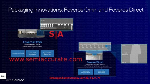
Meet the new Foveros twins, Omni and Direct
Omni is a bit murky but it looks to allow direct power to the top die via pillars beside the lower die rather than through vias in the lower die. This is a good thing in many ways but there is a huge challenge in getting the heights of all the pieces and the side columns even. The benefits are obvious, the engineering challenges are not even though they are substantial.
Foveros Direct is a bit simpler to explain, it takes two die and bonds their copper bumps/pillars directly to each other without solder. This saves a lot of steps and potentially ups yields. While Intel didn’t explicitly say how this is accomplished, it likely takes advantage of copper pillars bonding to itself at this scale when simply placed together. If so it is a really elegant way to do stack chips that saves money, ups yield, and simplifies everything.
That brings us to the second elephant hiding in the room, packaging and volume. Intel loves to claim leadership in advanced packaging but any cold hard look at the results seems to indicate otherwise. Intel surely talks the loudest in public but those developing similar tech, TSMC/Foundries and OSATs, have little incentive to go public with their developments. Their customers are known and engaged long ago, shouting will only tip off the competition. This isn’t to say anyone is ahead or behind, just don’t judge the landscape on who shouts loudest when one side isn’t talking. See AMD’s 3D V-Cache surprise at Computex for more on this.
The actual elephant is in volume. AMD has put out advanced packaging products for years at consumer volumes and at consumer price points. No we don’t mean Epyc/Ryzen, that is a half-step towards what SemiAccurate considers advanced packaging. What we mean are GPUs like Fiji and others with HBM, they were made in volume and priced at consumer price points. Xilinx was ahead of everyone with their Virtex-7 HT in 2012 though, and while that hit the volume mark, it didn’t really jump the consumer price point bar. That said it was not a consumer product so…
Going back to Intel’s efforts with Foveros and even EMIB, they had parts at consumer price points, sort of, none had actual chips for sale with MSRPs, just to OEMs. These all were scarce, short lived, and never came close to anything we consider consumer volumes. For low volume science experiments or PR exercises, price does not necessarily reflect cost of manufacturing, volume is more of a first order indicator. For products like Lakefield, Kaby Lake + AMD GPU, and several Altera FPGAs with EMIB, there was a lot of talk but little to no product on the market. Those that did come out were quickly EOLed and no follow on products with similar tech replaced them. So that brings us to the question of Intel’s tech itself, it is really interesting and has many useful advances, but can they make it in volume? Again time will tell.
The End of The Beginning:
So where do today’s announcements leave us? Intel is putting billions of dollars into a foundry effort with lots of tech and roadmap advances to back it all up. They are serious about being a foundry, no question there, but will customers take their word on anything at this point? The corpses littering the road behind seem to indicate that this is going to be a long slow slog uphill but SemiAccurate is cautiously optimistic that Intel’s new management is turning the ship. There are a lot of listed partners but is anyone putting a serious project on the line at the moment?
On the process naming front we have not one but three changes. The renaming of 10+++/SuperFin+ to 7nm is abjectly stupid and an unforced error that poisons the rest of the changes. 7nm -> 4nm could be warranted as could 5nm -> 3nm but since it all goes to Angstroms after, was there a point? Intel should have left SuperFin+ alone and moved everything else to Angstroms, it would have been a PR benefit instead of several steps backward.
The underlying tech looks impressive though, PowerVia is a really good thing, RibbonFET is the future, and the new Foveros twins are useful in different ways. Slides and proclamations are one thing, manufacturing at volume is another and Intel is far from digging out of that particular hole. The yearly cadence of new processes claim is plausible but a bit optimistic, we think Intel is still using several best case dates as ‘start of’ rather than the old way of actual availability. If this is the worst of the technical messaging sins it means Intel is moving in the right direction fast. Hopefully by the next disclosure they will be back to the old Intel way.
So can they do what they claim? Probably not exactly, nothing in tech goes perfectly well but the roadmaps laid out are the most plausible they have been in the better part of a decade. Several data points SemiAccurate is aware of line up with the high level items mentioned so that is a positive. If it can be made in volume at viable yields, Intel will be back. Lets hope they are, the industry needs more competition.S|A
Charlie Demerjian
Latest posts by Charlie Demerjian (see all)
- Qualcomm Is Cheating On Their Snapdragon X Elite/Pro Benchmarks - Apr 24, 2024
- What is Qualcomm’s Purwa/X Pro SoC? - Apr 19, 2024
- Intel Announces their NXE: 5000 High NA EUV Tool - Apr 18, 2024
- AMD outs MI300 plans… sort of - Apr 11, 2024
- Qualcomm is planning a lot of Nuvia/X-Elite announcements - Mar 25, 2024